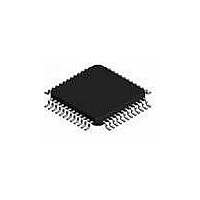
L6711TR STMicroelectronics, L6711TR Datasheet - Page 18

L6711TR
Manufacturer Part Number
L6711TR
Description
IC CTRLR 3PHASE VID/DACS 48-TQFP
Manufacturer
STMicroelectronics
Type
Step-Down (Buck)r
Datasheet
1.L6711TR.pdf
(50 pages)
Specifications of L6711TR
Internal Switch(s)
No
Synchronous Rectifier
No
Number Of Outputs
1
Voltage - Output
0.8 ~ 1.55 V
Current - Output
2A
Frequency - Switching
150kHz
Voltage - Input
12V
Operating Temperature
0°C ~ 70°C
Mounting Type
Surface Mount
Package / Case
48-TQFP Exposed Pad, 48-eTQFP, 48-HTQFP, 48-VQFP
Power - Output
2.5W
Output Voltage
0.8 V to 1.581 V
Output Current
95 A
Input Voltage
13.8 V
Mounting Style
SMD/SMT
Maximum Operating Temperature
+ 125 C
Minimum Operating Temperature
0 C
Lead Free Status / RoHS Status
Lead free / RoHS Compliant
Other names
497-5363-2
L6711TR
L6711TR
Available stocks
Company
Part Number
Manufacturer
Quantity
Price
Device description
6
18/50
Device description
The device is a three phase PWM controller with embedded high current drivers that
provides complete control logic and protections for a high performance step-down DC-DC
voltage regulator optimized for advanced microprocessor power supply. Multi phase buck is
the simplest and most cost-effective topology employable to satisfy the increasing current
demand of newer microprocessors and modern high current DC/DC converters and POLs. It
allows distributing equally load and power between the phases using smaller, cheaper and
most common external power mosfets and inductors. Moreover, thanks to the 120° of phase
shift between each phase, the input and output capacitor count results in being reduced.
Phase interleaving causes in fact input rms current and output ripple voltage reduction and
show an effective output switching frequency increase: the 150kHz free-running frequency
per phase, externally adjustable through a resistor, results tripled on the output.
The controller includes multiple DACs, selectable through an apposite pin (VID_SEL),
allowing compatibility with both VRD 10.x and Hammer specifications, also performing D-
VID transitions accordingly. The output voltage can be precisely selected, programming the
VID and VID_SEL pins, from 0.8185V to 1.5810V with 12.5mV binary steps (VRD 10.x
compliant mode - 6 BIT with -19mV offset already programmed during production) or from
0.800V to 1.550V with 25mV steps (VRM Hammer compliant mode - 5 BIT, VID5 programs
a 25mV positive offset in this case), with a maximum tolerance on the output regulated
voltage of ±0.5% (±0.6% for Hammer) over temperature and line voltage variations.
The device permits easy and flexible system design by allowing current reading across
either inductor or low side mosfet in fully differential mode simply selecting the desired way
through the CS_SEL pin. In both cases, also a sense resistor in series to the related
element can be considered to improve reading precision. The current information read
corrects the PWM output in order to equalize the average current carried by each phase
limiting the error at ±3% over static and dynamic conditions unless considering the sensing
element spread.
The device provides a programmable Over-Voltage protection to protect the load from
dangerous over stress and can be externally set to a fixed voltage through an apposite
resistor or it can be set internally with a fixed percentage, latching immediately by turning
ON the lower driver and driving high the FAULT pin. Furthermore, preliminary OVP
protection also allows the device to protect load from dangerous OVP when VCC is not
above the UVLO threshold.
Over-Current protection provided, with an OC threshold for each phase, causes the device
to enter in constant current mode until the latched UVP. Depending on the reading mode
selected, the device keeps constant the peak (inductor sensing) or the valley (LS sensing)
of the inductor current ripple.
The device drives high the FAULT pin after each latching event: to recover it is enough to
cycle VCC or the OUTEN pin.
A compact 7x7mm body TQFP48 package with exposed thermal pad allows dissipating the
power to drive the external mosfet through the system board.
L6711


