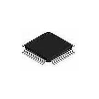
L6711TR STMicroelectronics, L6711TR Datasheet - Page 38

L6711TR
Manufacturer Part Number
L6711TR
Description
IC CTRLR 3PHASE VID/DACS 48-TQFP
Manufacturer
STMicroelectronics
Type
Step-Down (Buck)r
Datasheet
1.L6711TR.pdf
(50 pages)
Specifications of L6711TR
Internal Switch(s)
No
Synchronous Rectifier
No
Number Of Outputs
1
Voltage - Output
0.8 ~ 1.55 V
Current - Output
2A
Frequency - Switching
150kHz
Voltage - Input
12V
Operating Temperature
0°C ~ 70°C
Mounting Type
Surface Mount
Package / Case
48-TQFP Exposed Pad, 48-eTQFP, 48-HTQFP, 48-VQFP
Power - Output
2.5W
Output Voltage
0.8 V to 1.581 V
Output Current
95 A
Input Voltage
13.8 V
Mounting Style
SMD/SMT
Maximum Operating Temperature
+ 125 C
Minimum Operating Temperature
0 C
Lead Free Status / RoHS Status
Lead free / RoHS Compliant
Other names
497-5363-2
L6711TR
L6711TR
Available stocks
Company
Part Number
Manufacturer
Quantity
Price
Oscillator
15
38/50
Oscillator
The internal oscillator generates the triangular waveform for the PWM charging and
discharging with a constant current an internal capacitor. The switching frequency for each
channel, F
load side results in being tripled.
The current delivered to the oscillator is typically 25 A (corresponding to the free running
frequency Fsw=150kHz) and it may be varied using an external resistor (R
between the OSC pin and SGND or VCC (or a fixed voltage greater than 1.24V). Since the OSC
pin is fixed at 1.24V, the frequency is varied proportionally to the current sunk (forced) from (into)
the pin considering the internal gain of 6KHz/ A.
In particular connecting R
pin), while connecting R
pin), according to the following relationships:
Maximum programmable switching frequency depends on the Current Reading Method
selected. When reading across LS mosfet, the maximum switching frequency per phase
must be limited to 500kHz to avoid current reading errors causing, as a consequence,
current sharing errors. When reading across the inductor, higher switching frequency can be
approached (device power dissipation must be checked prior to design high switching
frequency systems).
Figure 19. R
R
R
OSC
OSC
14000
12000
10000
8000
6000
4000
2000
R
vs. GND: F
vs. 12V: F
OSC
0
25
[k ] to 12V vs. Selected F
SW
, is internally fixed at 150kHz so that the resulting switching frequency at the
50
OSC
SW
SW
vs. switching frequency
75
=
=
150kHz
150kHz
OSC
100
OSC
to VCC=12V the frequency is reduced (current is forced into the
SW
+
to SGND the frequency is increased (current is sunk from the
125
+
--------------------------- - 6
R
[kHz]
12-1.237
--------------------------- - 6
R
OSC
OSC
1.237
150
k
k
kHz
---------- -
kHz
---------- -
A
A
=
=
1000
150kHz
R
800
600
400
200
150kHz
OSC
0
150
[k ] to SGND vs. Selected F
250
+
+
6.457 10
---------------------------- -
R
7.422 10
---------------------------- -
R
OSC
350
OSC
k
450
k
7
6
OSC
550
) connected
650
SW
[kHz]
750
850
L6711


