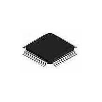
L6711TR STMicroelectronics, L6711TR Datasheet - Page 44

L6711TR
Manufacturer Part Number
L6711TR
Description
IC CTRLR 3PHASE VID/DACS 48-TQFP
Manufacturer
STMicroelectronics
Type
Step-Down (Buck)r
Datasheet
1.L6711TR.pdf
(50 pages)
Specifications of L6711TR
Internal Switch(s)
No
Synchronous Rectifier
No
Number Of Outputs
1
Voltage - Output
0.8 ~ 1.55 V
Current - Output
2A
Frequency - Switching
150kHz
Voltage - Input
12V
Operating Temperature
0°C ~ 70°C
Mounting Type
Surface Mount
Package / Case
48-TQFP Exposed Pad, 48-eTQFP, 48-HTQFP, 48-VQFP
Power - Output
2.5W
Output Voltage
0.8 V to 1.581 V
Output Current
95 A
Input Voltage
13.8 V
Mounting Style
SMD/SMT
Maximum Operating Temperature
+ 125 C
Minimum Operating Temperature
0 C
Lead Free Status / RoHS Status
Lead free / RoHS Compliant
Other names
497-5363-2
L6711TR
L6711TR
Available stocks
Company
Part Number
Manufacturer
Quantity
Price
Layout guidelines
18
18.1
44/50
Layout guidelines
Since the device manages control functions and high-current drivers, layout is one of the
most important things to consider when designing such high current applications.
A good layout solution can generate a benefit in lowering power dissipation on the power
paths, reducing radiation and a proper connection between signal and power ground can
optimize the performance of the control loops.
Integrated power drivers reduce components count and interconnections between control
functions and drivers, reducing the board space.
Here below are listed the main points to focus on when starting a new layout and rules are
suggested for a correct implementation.
Power connections.
These are the connections where switching and continuous current flows from the input
supply towards the load. The first priority when placing components has to be reserved to
this power section, minimizing the length of each connection and loop as much as possible.
To minimize noise and voltage spikes (EMI and losses) these interconnections must be a
part of a power plane and anyway realized by wide and thick copper traces: loop must be
anyway minimized. The critical components, i.e. the power transistors, must be located as
close as possible one to the other.
Figure 23
input capacitance (C
placed close to the power section in order to eliminate the stray inductance generated by
the copper traces. Low ESR and ESL capacitors are preferred.
Use as much VIAs as possible when power traces have to move between different planes
on the PCB: this reduces both parasitic resistance and inductance. Moreover, reproducing
the same high-current trace on more than one PCB layer will reduce the parasitic resistance
associated to that connection.
Connect output bulk capacitor as near as possible to the load, minimizing parasitic
inductance and resistance associated to the copper trace also adding extra decoupling
capacitors along the way to the load when this results in being far from the bulk capacitor
bank.
Figure 23. Power connections and related connections layout guidelines (same for
UGATEx
PHASEx
LGATEx
PGNDx
a. PCB power and ground planes areas
shows the details of the power connections involved and the current loops. The
all phases).
IN
), or at least a portion of the total capacitance needed, has to be
C
V
IN
IN
L
LOAD
PHASEx
BOOTx
SGND
VCC
To limit C
b. PCB small signal components placement
BOOT
Extra-Charge
+Vcc
V
C
IN
IN
L
LOAD
L6711


