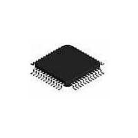
L6711TR STMicroelectronics, L6711TR Datasheet - Page 7

L6711TR
Manufacturer Part Number
L6711TR
Description
IC CTRLR 3PHASE VID/DACS 48-TQFP
Manufacturer
STMicroelectronics
Type
Step-Down (Buck)r
Datasheet
1.L6711TR.pdf
(50 pages)
Specifications of L6711TR
Internal Switch(s)
No
Synchronous Rectifier
No
Number Of Outputs
1
Voltage - Output
0.8 ~ 1.55 V
Current - Output
2A
Frequency - Switching
150kHz
Voltage - Input
12V
Operating Temperature
0°C ~ 70°C
Mounting Type
Surface Mount
Package / Case
48-TQFP Exposed Pad, 48-eTQFP, 48-HTQFP, 48-VQFP
Power - Output
2.5W
Output Voltage
0.8 V to 1.581 V
Output Current
95 A
Input Voltage
13.8 V
Mounting Style
SMD/SMT
Maximum Operating Temperature
+ 125 C
Minimum Operating Temperature
0 C
Lead Free Status / RoHS Status
Lead free / RoHS Compliant
Other names
497-5363-2
L6711TR
L6711TR
Available stocks
Company
Part Number
Manufacturer
Quantity
Price
L6711
2
2.1
Table 1.
Figure 4.
N°
1
2
3
4
5
6
7
VCCDR1
OFFSET
LGATE1
PGND1
COMP
SGND
Name
VCC
Pins description and connection diagrams
Pin descriptions
Pins description
Pins connection (top view)
Channel 1 LS driver supply: it can be varied from 5V to 12V buses.
It must be connected together with other VCCDRx pins.
Filter locally with at least 1 F ceramic cap vs. PGND1.
Channel 1 LS driver output.
A little series resistor helps in reducing device-dissipated power.
Channel 1 LS driver return path.
Connect to Power Ground Plane.
Device supply voltage. The operative supply voltage is 12V ±15%.
Filter with 1 F capacitor (Typ.) vs. SGND.
All the internal references are referred to this pin. Connect it to the PCB signal ground.
Offset programming pin, internally fixed at 1.240V.
Short to SGND to disable the offset generation or connect through a resistor R
SGND to program an offset (positive or negative, depending on TC status) to the regulated
output voltage as reported in the relative section.
This pin is connected to the error amplifier output and is used to compensate the control
feedback loop.
VCCDR3
VCCDR2
PHASE2
PHASE1
UGATE2
UGATE1
LGATE2
PGND2
BOOT2
BOOT1
N.C.
N.C.
37
38
39
40
41
42
43
44
45
46
47
48
36 35 34 33 32 31 30 29 28 27 26 25
1
2
3
4
5
L6711
6
7
8
Description
9 10 11 12
Pins description and connection diagrams
24
23
22
21
20
19
18
17
16
15
14
13
VID0
VID5
OSC / FAULT
CS_SEL
TC
CS3+
CS3-
CS2+
CS2-
CS1+
CS1-
OUTEN
OFFSET
to
7/50


