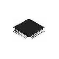
L6711TR STMicroelectronics, L6711TR Datasheet - Page 27

L6711TR
Manufacturer Part Number
L6711TR
Description
IC CTRLR 3PHASE VID/DACS 48-TQFP
Manufacturer
STMicroelectronics
Type
Step-Down (Buck)r
Datasheet
1.L6711TR.pdf
(50 pages)
Specifications of L6711TR
Internal Switch(s)
No
Synchronous Rectifier
No
Number Of Outputs
1
Voltage - Output
0.8 ~ 1.55 V
Current - Output
2A
Frequency - Switching
150kHz
Voltage - Input
12V
Operating Temperature
0°C ~ 70°C
Mounting Type
Surface Mount
Package / Case
48-TQFP Exposed Pad, 48-eTQFP, 48-HTQFP, 48-VQFP
Power - Output
2.5W
Output Voltage
0.8 V to 1.581 V
Output Current
95 A
Input Voltage
13.8 V
Mounting Style
SMD/SMT
Maximum Operating Temperature
+ 125 C
Minimum Operating Temperature
0 C
Lead Free Status / RoHS Status
Lead free / RoHS Compliant
Other names
497-5363-2
L6711TR
L6711TR
Available stocks
Company
Part Number
Manufacturer
Quantity
Price
L6711
The ITS circuit subtracts from the I
temperature as follow (see
considered):
where
where A and B are positive constants depending on the value of the external resistor R
(see
sensing element) temperature.
The resistor R
voltage at a fixed current as follow:
obtaining the following relationship:
where R
obtainable from
Figure
Controller (it results K
sensing element. Since R
iterative process is required to properly design the R
nature of the thermal sensor, a negative offset is needed to compensate the native offset
introduced by the ITS at a referenced temperature Tref and it is obtainable by connecting a
R
To disable this function, short the pin to SGND.
Figure 12. Integrated thermal sensor constant vs. external resistor R
V
–
I
OFFSET
R
OUT
OFFSET
FB
650
625
600
575
550
525
500
475
450
Figure
T,I
R
------------------------------------------------------------------ - I
I
12, k
TC
0
SENSE
SENSE
OUT
=
resistor between the OFFSET pin and SGND as follow:
T
10 20 30 40 50 60 70 80 90 100
–
T
I
J
12), T
TC
is the Temperature Coupling Coefficient between the sensing element and the
=
TC
=
is the sensing element resistance value (at T
T
VID R
Rg
---------- -
R
can be designed in order to zero the temperature influence on the output
ref
J
1
TC
T
is the device junction temperature and T
A [mV] vs. R
–
MOS
=
T
A
A
--------------------------------------------- -
FB
= (T
–
+
+
TC
25
B
B
Figure
J
R
----------------------------------------- - I
depends from the constant B depending in turn from R
-25)/(T
TC
R
SEN SE
T
T
TC
[K ]
OUT
J
ref
–
Rg
11, Only the I
–
FB
25
R
+
MOS
25
T
TC
current a current proportional to the sensed
---------- - B
R
R
MOS
FB
TC
-25)) and
=
---------------------
R
SENSE
OUT
Rg
T
DROOP
2.00
1.90
1.80
1.70
1.60
1.50
J
–
–
I
25
TC
--------------------
0
is the Temperature Coefficient of the
TC
B k
T
I
and I
10 20 30 40 50 60 70 80 90 100
=
OUT
value. As a consequence of the
J
B [mV/°C] vs. R
T
0
TC
MOS
MOS
contributes to I
= 25ºC), B is the constant
is the mosfet (or the used
TC
[K ]
Voltage positioning
TC
FB
have been
TC
, an
27/50
TC


