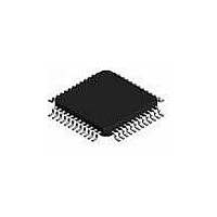
L6711TR STMicroelectronics, L6711TR Datasheet - Page 35

L6711TR
Manufacturer Part Number
L6711TR
Description
IC CTRLR 3PHASE VID/DACS 48-TQFP
Manufacturer
STMicroelectronics
Type
Step-Down (Buck)r
Datasheet
1.L6711TR.pdf
(50 pages)
Specifications of L6711TR
Internal Switch(s)
No
Synchronous Rectifier
No
Number Of Outputs
1
Voltage - Output
0.8 ~ 1.55 V
Current - Output
2A
Frequency - Switching
150kHz
Voltage - Input
12V
Operating Temperature
0°C ~ 70°C
Mounting Type
Surface Mount
Package / Case
48-TQFP Exposed Pad, 48-eTQFP, 48-HTQFP, 48-VQFP
Power - Output
2.5W
Output Voltage
0.8 V to 1.581 V
Output Current
95 A
Input Voltage
13.8 V
Mounting Style
SMD/SMT
Maximum Operating Temperature
+ 125 C
Minimum Operating Temperature
0 C
Lead Free Status / RoHS Status
Lead free / RoHS Compliant
Other names
497-5363-2
L6711TR
L6711TR
Available stocks
Company
Part Number
Manufacturer
Quantity
Price
L6711
14.5
14.5.1
Low side sense overcurrent (CS_SEL=OPEN)
The device detects an Over Current condition for each phase when the current information
I
keeps the relative LS mosfet on, skipping clock cycles, until the threshold is crossed back
and IINFOx results being lower than the I
the bottom of each inductor current ripple.
After exiting the OC condition, the LS mosfet is turned off and the HS is turned on with a
duty cycle driven by the PWM comparator.
Keeping the LS on, skipping clock cycles, causes the on-time subsequent to the exit from
the OC condition to increase. Considering now that the device, with this kind of current
sense, has maximum on-time dependence with the delivered current given by the following
relationship:
Where I
=1/F
This linear dependence has a value at zero load of 0.80 ·T
0.40 ·T
This happens when the maximum ON time is reached before that the current in each phase
reaches IO
is able to regulate considering the T
desired output characteristic crosses the T
resulting voltage will start to drop after the crossing.
In this case, the device doesn't perform constant current limitation but only limits the
maximum ON time following the previous relationship. The output voltage starts to decrease
follows the resulting characteristic (dotted in
I
Figure 17. TON limited operation
T
T
INFOx
DROOP
ON,MAX
ON
SW
Limited output voltage.
overcomes the fixed threshold of I
SW
).
=105 A.
OUT
0 . 8 0 · V
0 . 4 0 · V
=
typical and results in two different over current behaviors of the device:
V
CPx
O U T
0.80 I
is the output current (I
I N
I N
(I
INFOx
Maximum output Voltage
–
D ROOP
<I
OCTH
T
O N
L i m i t e d O u t p u t
3.8k
c h a r a c t e r i s t i c
( I
D R O O P
).
I
O
C P
Figure 17
= 3 · I
= 1 0 5A )
O C P x
T
SW
OUT
ON
I
O U T
=
= ·I
limitation imposed by the previous relationship. If the
⎧
⎪
⎨
⎪
⎩
OCTH
shows the maximum output voltage that the device
OCTH
0.80 T
0.40 T
ON
PHASEx
Figure
(35 A Typ). When this happens, the device
limited maximum output voltage, the output
threshold. This implies that the device limits
0 . 8 0 · V
0 . 4 0 · V
SW
SW
b) TON Limited Output Voltage
Output voltage monitor and protections
) and T
V
O U T
17) until UVP is detected or anyway until
I N
I N
I
I
DROOP
DROOP
SW
SW
is the switching period (T
=
=
and at maximum current of
0 A
105 A
( I
D R O O P
I
O C P
= 3 · I
= 1 0 5A )
O C P x
c h a r a c t e r i s t i c
R e s u l t i n g O u t p u t
c h a r a c t e r i s t i c
D e s i r e d O u t p u t
U V P t h r e s h o l d
I
O U T
a n d
SW
35/50


