L6711TR STMicroelectronics, L6711TR Datasheet - Page 42

L6711TR
Manufacturer Part Number
L6711TR
Description
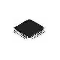
IC CTRLR 3PHASE VID/DACS 48-TQFP
Manufacturer
STMicroelectronics
Type
Step-Down (Buck)r
Datasheet
1.L6711TR.pdf
(50 pages)
Specifications of L6711TR
Internal Switch(s)
No
Synchronous Rectifier
No
Number Of Outputs
1
Voltage - Output
0.8 ~ 1.55 V
Current - Output
2A
Frequency - Switching
150kHz
Voltage - Input
12V
Operating Temperature
0°C ~ 70°C
Mounting Type
Surface Mount
Package / Case
48-TQFP Exposed Pad, 48-eTQFP, 48-HTQFP, 48-VQFP
Power - Output
2.5W
Output Voltage
0.8 V to 1.581 V
Output Current
95 A
Input Voltage
13.8 V
Mounting Style
SMD/SMT
Maximum Operating Temperature
+ 125 C
Minimum Operating Temperature
0 C
Lead Free Status / RoHS Status
Lead free / RoHS Compliant
Other names
497-5363-2
L6711TR
L6711TR
Available stocks
Company
Part Number
Manufacturer
Quantity
Price
System control loop compensation
42/50
Removing the dependence from the Error Amplifier gain, so assuming this gain high
enough, the control loop gain results:
With further simplifications, it results:
Considering now that in the application of interest it can be assumed that Ro>>R
ESR<<Ro and R
The ACM control loop gain is designed to obtain a high DC gain to minimize static error and
cross the 0dB axes with a constant -20dB/dec slope with the desired crossover frequency
Both the poles are fixed once the output filter is designed and the zero is fixed by ESR and
the Droop resistance.
To obtain the desired shape an R
implementation. A zero at
integrator minimizes the static error while placing the zero in correspondence with the L-C
resonance a simple -20dB/dec shape of the gain is assured).
In fact, considering the usual value for the output filter, the LC resonance results to be at
frequency lower than the above reported zero.
Compensation network can be simply designed placing
over frequency
G
G
G
R
T
F
LOOP
LOOP
LOOP
. Neglecting the effect of Z
=
amplitude and has a typical value of 3V
PWM
R
--------------------------------- -
C
FB
s
s
s
F
=
V
=
=
=
=
I N
------------------- -
V
–
–
–
4
-- -
5
4
-- -
5
4
-- -
5
4
-- -
5
Co
OSC
R
F
---------------
------------------
------------------
------------------
DROO
T
V
V
V
V
V
L
-- -
3
V
V
V
IN
as desired obtaining:
osc
5
-- -
4
OSC
OSC
OSC
I N
I N
I N
P<<Ro, it results:
is the PWM transfer function where V
T
----------------------------------- -
Z
Z
--------------
Z
--------------
R
R
P
F
F
------------------------------------------------------ -
3
FB
FB
s
s
s
F
Z
F
=1/R
R
F
(s), the transfer function has one zero and two poles.
+
DROOP
Ro
------------------------------------ -
---------------------------------------------------------------------------------------------------------------------------------
s
s
Z
2
L
F
Ro
-C
F
+
Co
L
s
C
R
F
F
+
DROOP
+
series network is considered for the Z
⎛
is then introduced together with an integrator. This
R
------ -
L
-- -
3
Rs
------- -
Rg
3
ESR
1
L
+
+
s
+
s Co
---------------------------------------------------------------------------------------------------------------------------------
s
Z
-------------- -
R
2
P
---------------
3 Ro
FB
Co
s
L
⎞
⎠
R
1
+
L
-- -
3
D ROOP
+
Co ESR
+
s Co
s
Z
=
---------------
3 Ro
+
L
ESR
LC
OSC
R
+
DROOP
Co
and imposing the cross-
+
is the oscillator ramp
Co ESR
R
------ -
3
//Ro
L
+
1
+
+
ESR
F
(s)
Co
L
R
------ -
;
3
L
L6711
+
1


