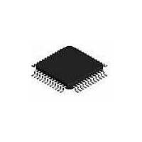
L6711TR STMicroelectronics, L6711TR Datasheet - Page 34

L6711TR
Manufacturer Part Number
L6711TR
Description
IC CTRLR 3PHASE VID/DACS 48-TQFP
Manufacturer
STMicroelectronics
Type
Step-Down (Buck)r
Datasheet
1.L6711TR.pdf
(50 pages)
Specifications of L6711TR
Internal Switch(s)
No
Synchronous Rectifier
No
Number Of Outputs
1
Voltage - Output
0.8 ~ 1.55 V
Current - Output
2A
Frequency - Switching
150kHz
Voltage - Input
12V
Operating Temperature
0°C ~ 70°C
Mounting Type
Surface Mount
Package / Case
48-TQFP Exposed Pad, 48-eTQFP, 48-HTQFP, 48-VQFP
Power - Output
2.5W
Output Voltage
0.8 V to 1.581 V
Output Current
95 A
Input Voltage
13.8 V
Mounting Style
SMD/SMT
Maximum Operating Temperature
+ 125 C
Minimum Operating Temperature
0 C
Lead Free Status / RoHS Status
Lead free / RoHS Compliant
Other names
497-5363-2
L6711TR
L6711TR
Available stocks
Company
Part Number
Manufacturer
Quantity
Price
Output voltage monitor and protections
14.4
34/50
Figure 16. Output voltage protections and typical principle connections to assure
Over current
Depending on the current reading method selected, the device limits the peak or the bottom
of the inductor current entering in constant current until setting UVP as below explained.
The Over Current threshold has to be programmed, by designing the Rg resistors, to a safe
value, in order to be sure that the device doesn't enter OCP during normal operation of the
device. This value must take into consideration also the extra current needed during the
Dynamic VID Transition I
DCR, the process spread and temperature variations of these sensing elements.
Moreover, since also the internal threshold spreads, the Rg design must consider its
minimum value I
where I
Quasi Constant Current (LS Mosfet Sense) or Constant Current (Inductor Sense), I
must be calculated starting from the corresponding output current value I
(I
where I
Current (LS Mosfet Sense) or Constant Current (Inductor Sense), I
ripple in each phase and I
In particular, since the device limits the peak or the valley of the inductor current (according
to CS_SEL status), the ripple entity, when not negligible, impacts on the real OC threshold
value and must be considered.
Rg
I
OCPx
D-VID
PreOVP TurnON
=
I
-------------------------------------------------------------------- -
=
Vcc TurnON
OCPx max
must also be considered when D-VID are implemented):
OCP
OUT(OCP)
⎧
⎪
⎪
⎨
⎪
⎪
⎩
I
-------------------------- -
I
-------------------------- -
OUT OCP
OUT OCP
x is the current measured by the current reading circuitry when the device enters
complete protection.
I
V cc
OC TH min
3
3
OCTH(min)
is still the output current value at which the device enters Quasi Constant
R
Preliminary OVP
FBR Monitored
(OUTEN = 0)
SENSE max
–
+
---------- -
---------- -
I
2
I
2
pp
pp
Preliminary OVP Enabled
D-VID
D-VID
as follow:
+
+
FBR Monitored
No Protection
I
-------------- Low Side Mosfet Sense
I
-------------- Inductor DCR Sense
D -VID
D-VID
Provided
3
3
and, since the device reads across mosfets R
is the additional current required by D-VID (when applicable).
Programmable OVP
VSEN Monitored
(OUTEN = 1)
+5V
+12V
SB
PP
is the inductor current
OUT(OCP)
VCC
VCCDR1
VCCDR2
VCCDR3
dsON
or inductor
as follow
OCPx
L6711


