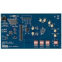
AD9551/PCBZ Analog Devices Inc, AD9551/PCBZ Datasheet - Page 19

AD9551/PCBZ
Manufacturer Part Number
AD9551/PCBZ
Description
BOARD EVAL FOR AD9951
Manufacturer
Analog Devices Inc
Datasheet
1.AD9551PCBZ.pdf
(40 pages)
Specifications of AD9551/PCBZ
Main Purpose
Timing, Clock Generator
Embedded
No
Utilized Ic / Part
AD9551
Primary Attributes
2 Inputs, 2 Outputs, VCO
Secondary Attributes
Graphical User Interface, USB Interface
Silicon Manufacturer
Analog Devices
Application Sub Type
Clock Generator
Kit Application Type
Clock & Timing
Silicon Core Number
AD9551
Kit Contents
Board
Lead Free Status / RoHS Status
Lead free / RoHS Compliant
Input PLL
The input PLL consists of a phase/frequency detector (PFD),
a digital loop filter, and a digitally controlled crystal oscillator
(DCXO) that operates in a closed loop. The loop contains a 2×
frequency multiplier, a 2× frequency divider, a 5× divider that
has a dedicated SDM, and switching logic, as shown in Figure 20.
The input PLL has a digital loop filter with a loop bandwidth of
approximately 180 Hz. This relatively narrow loop bandwidth
gives the AD9551 the ability to suppress jitter appearing on the
input references (REFA and REFB). By default, the sample rate
of the digital loop filter is f
input reference after it is scaled down by the input divider). This
yields a loop response with peaking of typically <0.2 dB. For appli-
cations that can benefit from a reduced acquisition time but can
tolerate more peaking (~0.5 dB), the user can increase the sample
rate of the loop filter to f
The configuration of the input PLL depends on the state of the
frequency selection pins, which establishes whether the device
operates in the normal mode or the 19.44 MHz mode. The con-
figuration of the input PLL also depends on the state of the 2×
frequency multiplier bit (Register 0x1D[2]) and the state of the
2× frequency divider bit (Register 0x33[6]).
With the device in normal mode, the input PLL feedback signal
and the signal delivered to the output PLL are the same. In this
mode, the user has three options to scale the frequency at the
output of the DCXO.
•
•
•
To select the upconversion option, set Register 0x1D[2] to 1. To
select the downconversion option, set Register 0x33[6] to 1.
Note that setting Register 0x1D[2] to 1 renders Register 0x33[6]
ineffective (see Figure 20).
f
REF
Unity (default). The crystal frequency is the same as f
Frequency upconversion using the 2× multiplier: f
twice the crystal frequency
Frequency downconversion using the 2× divider: f
half the crystal frequency.
P
F
D
FILTER
LOOP
DIG.
19.44MHz MODE
DCXO
XTAL
Figure 20. Input PLL
REF
1
0
REF
via Register 0x33[7].
/8 (f
SDM
÷
2x
÷
2
5
REF
is the frequency of the active
1
0
REG. 0x1D[2]
0
1
19.44MHz MODE
REG. 0x33[6]
TO
OUTPUT
PLL
REF
REF
REF
is
.
is
Rev. B | Page 19 of 40
In all cases mentioned previously, the user must ensure that f
meets the required relationship relative to the crystal resonant
frequency. This is important because the narrow control range of
the DCXO requires close adherence to the required frequency
ratio (1/2, 1, or 2, depending on the selected option). Note, also,
that the frequency delivered to the output PLL is always the
same as f
When the device is in 19.44 MHz mode, the user must ensure
that f
the input PLL is different from that of normal mode. Specifically,
the feed-back signal and the signal delivered to the output PLL
are no longer the same. Instead, the device automatically configures
the feedback path to include the 2× frequency multiplier along
with a 5× divider coupled to a dedicated third-order SDM. The
device automatically sets the modulus of this SDM based on the
crystal frequency configured by Register 0x33[5:4]. This SDM also
has a built-in PRBS generator to randomize its output sequence.
Even though the device automatically configures the feedback
path in 19.44 MHz mode, the user can select the 2× multiplied or
2× divided output of the DCXO as the signal to the output PLL.
The 2× divider is in effect when Register 0x1D[2] = 0 (default).
The 2× multiplier is in effect when Register 0x1D[2] = 1. Note
that, unlike normal mode, the 19.44 MHz mode does not have
a unity option.
Using Register 0x1D[1] allows the user to bypass the entire input
PLL section. With the input PLL bypassed, the prescaled active
input reference signal (after synchronization) routes directly to the
PFD of the output PLL. However, even when the input PLL is
bypassed, the user must provide an external crystal so that the
DCXO is functional because the reference monitor and reference
synchronization blocks use the DCXO output as a clock source.
Output PLL
The output PLL consists of a phase-frequency detector (PFD),
a partially integrated analog loop filter (Figure 21), an integrated
voltage-controlled oscillator (VCO), and a feedback divider
with an optional third-order SDM that allows for fractional
divide ratios. The output PLL produces a nominal 3.7 GHz signal
that is phase-locked to the prescaled active input reference signal.
The PFD of the output PLL drives a charge pump that increases,
decreases, or holds constant the charge stored on the loop filter
capacitors (both internal and external). The stored charge results in
a voltage that sets the output frequency of the VCO. The feedback
loop of the PLL causes the VCO control voltage to vary in such
a way as to phase lock the PFD input signals.
CHARGE
FROM
PUMP
REF
= 19.44 MHz. In 19.44 MHz mode, the configuration of
LOOP FILTER
REF
CAPACITOR
EXTERNAL
in normal mode.
17
2.5kΩ
Figure 21. Internal Loop Filter
105pF
1.25kΩ
15pF
1.25kΩ
15pF
2.5kΩ
AD9551
20pF
TO
VCO
REF


