AD9551/PCBZ Analog Devices Inc, AD9551/PCBZ Datasheet - Page 22
AD9551/PCBZ
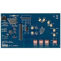
Manufacturer Part Number
AD9551/PCBZ
Description
BOARD EVAL FOR AD9951
Manufacturer
Analog Devices Inc
Datasheet
1.AD9551PCBZ.pdf
(40 pages)
Specifications of AD9551/PCBZ
Main Purpose
Timing, Clock Generator
Embedded
No
Utilized Ic / Part
AD9551
Primary Attributes
2 Inputs, 2 Outputs, VCO
Secondary Attributes
Graphical User Interface, USB Interface
Silicon Manufacturer
Analog Devices
Application Sub Type
Clock Generator
Kit Application Type
Clock & Timing
Silicon Core Number
AD9551
Kit Contents
Board
Lead Free Status / RoHS Status
Lead free / RoHS Compliant


AD9551
The value of K depends on the device configuration, as shown
in Table 16.
Table 16. Configuring the Value of K
Mode
19.44 MHz
Normal
The user must carefully consider the operating frequency of the
externally connected crystal resonator (assuming that the input
PLL is not bypassed). Because the DCXO is capable of pulling
the crystal over a 50 ppm range only, the output frequency of
the DCXO is essentially identical to the crystal frequency.
The denominator of Equation 1 is the input division factor, which
has an integer part (N
optional fractional part that is associated with the input SDM.
Note that when bypassing the SDM, the device forces the frac-
tional part to 0 (equivalent to FRAC
The numerator of Equation 2 contains the feedback division
factor, which has an integer part (N) due to an integer divider,
as well as an optional fractional part (FRAC/MOD) that is
associated with the feedback SDM.
Equation 1 and Equation 2, along with the constraints placed on
their variables, imply a rational relationship between f
That is, the ratio f
integers. For example, it is not possible to configure the device
to satisfy a frequency ratio having a value of −2 because it is
irrational (that is, not expressible as a ratio of two integers).
CALCULATING DIVIDER VALUES
This section provides a 5-step procedure for calculating the divider
values when given a specific f
described in general terms, but a specific example is provided
for clarity. The example assumes the use of the frequency control
pins with A[3:0] = 0010 and Y[3:0] = 0100 (see Table 13 and
Table 14). The example parameters are as follows:
1/2 + FRAC
f
f
f
REF
OUT1
IF
=
=
26
=
622
625
f
52 MHz
50 MHz
49.86 MHz
49.152 MHz
MHz
CRYSTAL
.
08
x
⎛
⎜
⎝
/(2 × MOD
OUT1
66
64
⎛
⎜
⎝
239
237 ⎠
⎞
⎟
⎠
/f
x
) due to an integer divider, as well as an
MHz
REF
⎞
⎟
MHz
must be expressible as a ratio of two
x
)
OUT1
K
1300/243
325/243
1250/243
625/486
277/54
277/216
2048/405
512/405
1
/f
x
REF
= −MOD
ratio. The methodology is
Description
Using 2× multiplier
Using 2× divider
Using 2× multiplier
Using 2× divider
Using 2× multiplier
Using 2× divider
Using 2× multiplier
Using 2× divider
Crystal independent
x
).
REF
and f
OUT1
Rev. B | Page 22 of 40
.
Calculation Steps
1.
2.
3.
Table 17. Combinations of P
P
4
4
5
5
6
7
8
9
10
0
Ensure that f
As shown in the following equation, f
as a ratio of two integers, so f
Determine the output divide factor (ODF).
Note that the VCO frequency (f
4050 MHz. The ratio, f
Given the specified value of f
range of f
must be an integer, which means that ODF = 6 (because 6
is the only integer between 5.2 and 6.3).
Determine suitable values for P
The ODF is the product of the two output dividers; that is,
ODF = P
for the given example. Therefore, we have P
constraints that P
(see the Output/Input Frequency Relationship section).
These constraints lead to the singular solution of P
= 1.
Although this particular example yields a singular solution
for the output divider values with f
f
one. For example, if f
34 to 40. This leads to an assortment of possible values for
P
The P
valid. However, note that they yield only three valid ODF
values (35, 36, and 40) from the original range of 34 to 40.
OUT1
f
0
f
OUT1
REF
and P
frequencies result in multiple ODFs rather than just
0
and P
=
1
0
622
VCO
, as shown in Table 17.
× P
625
, the ODF spans a range of 5.2 to 6.3. The ODF
1
.
OUT1
08
1
combinations listed in Table 17 are all equally
. It has already been determined that ODF = 6
⎛
⎜
⎝
P
9
10
7
8
6
5
5
4
4
⎛
⎜
⎝
64
66
1
0
239
237
and f
and P
⎞
⎟
⎠
OUT1
⎞
⎟
⎠
REF
VCO
=
1
are both integers and that 4 ≤ P
625
0
are rationally related.
/f
= 100 MHz, the ODF ranges from
62208
and P
OUT1
OUT1
OUT1
(
66
, indicates the required ODF.
and f
0
)(
VCO
(
(~644.53 MHz) and the
1
and P
OUT1
239
237
ODF
36
40
35
40
36
35
40
36
40
) spans 3350 MHz to
REF
)(
≈ 644.53 MHz, some
)(
OUT1
64
1
100
are rationally related.
.
)
/f
0
)
REF
× P
=
is expressible
977
951
1
= 6, with the
0
= 6, and P
,
,
625
553
,
,
568
0
000
≤ 11
1
Related parts for AD9551/PCBZ
Image
Part Number
Description
Manufacturer
Datasheet
Request
R


Part Number:
Description:
±1.7g Dual-Axis IMEMS Accelerometer Evaluation Board
Manufacturer:
Analog Devices Inc
Datasheet:

Part Number:
Description:
Inertial Sensor Evaluation System
Manufacturer:
Analog Devices Inc
Datasheet:
Part Number:
Description:
Manufacturer:
Analog Devices Inc
Datasheet:
Part Number:
Description:
Manufacturer:
Analog Devices Inc
Datasheet:
Part Number:
Description:
Manufacturer:
Analog Devices Inc
Datasheet:
Part Number:
Description:
Manufacturer:
Analog Devices Inc
Datasheet:
Part Number:
Description:
Manufacturer:
Analog Devices Inc
Datasheet:
Part Number:
Description:
Manufacturer:
Analog Devices Inc
Datasheet:
Part Number:
Description:
Manufacturer:
Analog Devices Inc
Datasheet:
Part Number:
Description:
Manufacturer:
Analog Devices Inc
Datasheet:
Part Number:
Description:
Manufacturer:
Analog Devices Inc
Datasheet:
Part Number:
Description:
Manufacturer:
Analog Devices Inc
Datasheet: