AD9551/PCBZ Analog Devices Inc, AD9551/PCBZ Datasheet - Page 20
AD9551/PCBZ
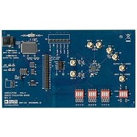
Manufacturer Part Number
AD9551/PCBZ
Description
BOARD EVAL FOR AD9951
Manufacturer
Analog Devices Inc
Datasheet
1.AD9551PCBZ.pdf
(40 pages)
Specifications of AD9551/PCBZ
Main Purpose
Timing, Clock Generator
Embedded
No
Utilized Ic / Part
AD9551
Primary Attributes
2 Inputs, 2 Outputs, VCO
Secondary Attributes
Graphical User Interface, USB Interface
Silicon Manufacturer
Analog Devices
Application Sub Type
Clock Generator
Kit Application Type
Clock & Timing
Silicon Core Number
AD9551
Kit Contents
Board
Lead Free Status / RoHS Status
Lead free / RoHS Compliant


AD9551
The gain of the output PLL is proportional to the current
delivered by the charge pump. The user can override the default
charge pump current setting, and, thereby, the PLL gain, by using
Register 0x0A[7:0].
The output PLL has a VCO with 128 frequency bands spanning
a range of 3350 MHz to 4050 MHz (3700 MHz nominal). How-
ever, the actual operating frequency within a particular band
depends on the control voltage that appears on the loop filter
capacitor. The control voltage causes the VCO output frequency
to vary linearly within the selected band. This frequency vari-
ability allows the control loop of the output PLL to synchronize
the VCO output signal with the reference signal applied to the
PFD. Typically, the device selects the appropriate band and adjusts
the signal level as part of its calibration process. However, the
user can force calibration by first enabling SPI control of VCO
calibration (Register 0x0E[2] = 1) and then writing a 1 to the
calibrate VCO bit (Register 0x0E[7]). To facilitate system debug-
ging, the user can override the VCO band setting by first
enabling SPI control of the VCO band (Register 0x0E[0] = 1)
and then writing the desired value to Register 0x10[7:1].
The output PLL has a feedback divider coupled with a third-order
SDM (similar to the REFA and REFB input dividers) that enables
the output PLL to provide integer-plus-fractional frequency up-
conversion. The integer factor, N, is variable from 0 to 255 via an
8-bit programming register. However, the minimum practical value
of N is 64 because this sufficiently reduces the VCO frequency
in the PLL feedback path to an acceptable range. The SDM in the
feedback path allows for a fractional divide value that takes the
form of N + F/M, where N is the integer part (eight bits), M is
the modulus (20 bits), and F is the fractional part (20 bits), with
all three parameters being positive integers. The feedback SDM
gives the AD9551 the ability to support a wide range of output
frequencies with exact frequency ratios relative to the input
reference.
PLL Locked Indicators
Both the input and output PLLs provide a status indicator that
appears at an external pin. The indicator shows when the PLL has
acquired a locked condition. The input PLL provides the INPUT
PLL LOCKED signal, and the output PLL provides the OUTPUT
PLL LOCKED signal.
Output Dividers
Three integer dividers exist in the output chain. The first divider
(P
second divider (P
integer submultiple of the output frequency of the P
The third divider (P
as an integer submultiple of the OUT1 frequency.
0
) yields an integer submultiple of the VCO frequency. The
1
) establishes the frequency at OUT1 as an
2
) establishes the output frequency at OUT2
0
divider.
Rev. B | Page 20 of 40
Output Drivers
The user has control over the following output driver parameters
via the programming registers:
•
•
•
•
The logic families are LVDS, LVPECL, and CMOS. Selection of
the logic family is via the mode control bits in the OUT1 driver
control register (Register 0x32[5:3]) and the OUT2 driver control
register (Register 0x34[5:3]), as detailed in Table 15. Regardless
of the selected logic family, each output driver uses two pins: OUT1
and OUT1 are used by one driver, and OUT2 and OUT2 are used
by the other. This enables support of the differential signals
associated with the LVDS and LVPECL logic families. CMOS,
on the other hand, is a single-ended signal requiring only one
output pin, but both output pins are available for optional pro-
vision of a dual, single-ended CMOS output clock. Refer to the first
entry (CMOS (both pins)) in
Table 15. Output Channel Logic Family and Pin Functionality
Mode
Control Bits[2:0]
000
001
010
011
100
101
110
111
If the mode bits indicate the CMOS logic family, the user has
control of the logic polarity associated with each CMOS output
pin via the OUT1 and OUT2 driver control registers.
If the mode bits indicate the CMOS or LVDS logic family, the
user can select whether the output driver uses weak or strong
drive capability via the OUT1 and OUT2 driver control registers.
In the case of the CMOS family, the strong setting allows for
driving increased capacitive loads. In the case of the LVDS family,
the nominal weak and strong drive currents are 3.5 mA and
7 mA, respectively.
The OUT1 and OUT2 driver control registers also have a power-
down bit to enable/disable the output drivers. The power-down
function is independent of the logic family selection.
Note that, unless the user programs the device to allow SPI port
control of the output drivers, the drivers default to LVPECL or
LVDS, depending on the logic level on the OUTSEL pin (Pin 16).
For OUTSEL = 0, both outputs are LVDS. For OUTSEL = 1, both
outputs are LVPECL. In the pin-selected LVDS mode, the user
can still control the drive strength, using the SPI port.
Logic family and pin functionality
Polarity (for CMOS family only)
Drive current
Power-down
Logic Family and Pin Functionality
CMOS (both pins)
CMOS (positive pin), tristate (negative pin)
Tristate (positive pin), CMOS (negative pin)
Tristate (both pins)
LVDS
LVPECL
Undefined
Undefined
Table 15
.
Related parts for AD9551/PCBZ
Image
Part Number
Description
Manufacturer
Datasheet
Request
R


Part Number:
Description:
±1.7g Dual-Axis IMEMS Accelerometer Evaluation Board
Manufacturer:
Analog Devices Inc
Datasheet:

Part Number:
Description:
Inertial Sensor Evaluation System
Manufacturer:
Analog Devices Inc
Datasheet:
Part Number:
Description:
Manufacturer:
Analog Devices Inc
Datasheet:
Part Number:
Description:
Manufacturer:
Analog Devices Inc
Datasheet:
Part Number:
Description:
Manufacturer:
Analog Devices Inc
Datasheet:
Part Number:
Description:
Manufacturer:
Analog Devices Inc
Datasheet:
Part Number:
Description:
Manufacturer:
Analog Devices Inc
Datasheet:
Part Number:
Description:
Manufacturer:
Analog Devices Inc
Datasheet:
Part Number:
Description:
Manufacturer:
Analog Devices Inc
Datasheet:
Part Number:
Description:
Manufacturer:
Analog Devices Inc
Datasheet:
Part Number:
Description:
Manufacturer:
Analog Devices Inc
Datasheet:
Part Number:
Description:
Manufacturer:
Analog Devices Inc
Datasheet: