AD9551/PCBZ Analog Devices Inc, AD9551/PCBZ Datasheet - Page 24
AD9551/PCBZ
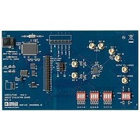
Manufacturer Part Number
AD9551/PCBZ
Description
BOARD EVAL FOR AD9951
Manufacturer
Analog Devices Inc
Datasheet
1.AD9551PCBZ.pdf
(40 pages)
Specifications of AD9551/PCBZ
Main Purpose
Timing, Clock Generator
Embedded
No
Utilized Ic / Part
AD9551
Primary Attributes
2 Inputs, 2 Outputs, VCO
Secondary Attributes
Graphical User Interface, USB Interface
Silicon Manufacturer
Analog Devices
Application Sub Type
Clock Generator
Kit Application Type
Clock & Timing
Silicon Core Number
AD9551
Kit Contents
Board
Lead Free Status / RoHS Status
Lead free / RoHS Compliant


AD9551
As in Step 4, use long division to convert the fraction, X/Y
to an integer, N, and a proper fraction, R/Y (R and Y a
integers). The same caution giv
regarding the need to use long division rather than a
calculator or a math program.
Given the example of X = 14,867,712 and Y = 616,200,
long division yields the following: N = 24 and R/Y =
78,912/616,200, which reduces to R/Y = 3,288/25,675. The
only caveats are that N must meet t
and N
section and t
Next, use R and Y to compute the following:
Q = 2 R − Y
Using R = 3288 and Y = 25,675 from
yields
Q = 2 × 3288 − 25,675 = −19,099
These va
divider values: N
25,675.
In the example, FRAC
an integer plus the fractional component, FRAC
This implies that the input SDM is necessary as part of the
input divider. If FRAC
an integer and the SDM is not required (it can be bypassed).
B
given in the Output/Input Frequency R
lues of N, Q, and Y constitute the respective input
hat Y < 2
x
= 24, FRAC
x
19
x
= 0, then the input division factor is
is nonzero, so the division value i
(524,288).
x
= −19,099, and MOD
en in Step 4 applies here,
he constraints for N
the previous example
elationship
x
/MOD
x
=
re
A
x
Rev. B | Page 24 of 40
.
s
,
LOW DROPOUT (LDO) REGULATORS
The AD9551 is powered from a single 3.3 V supply and contains
on-chip LDO regulators for each function to eliminate the need
for external LDOs. To ensure optimal performance, each LDO
output should have a 0.47 μF capacitor connected between its
access pin and ground.
Note that for best performance, the LDO bypass capacitors
must be placed in close proximity to the device.
The choice of MOD
input section in a manner similar to the feedback dividers.
However, the spectral spacing of the spurs for the input
SDMs is as follows:
The input SDMs are similar to the feedback SDM in that it
is desirable to scale MOD
2
viously in Step 5. In the example calculation, the value of
MOD
part of 2
results: FRAC
25,675×20 = 513,500.
However, these FRAC
those that appear in Table 13 (A[3:0] = 0010). The reason is
that a scale factor of 6 (instead of 20) was found to yield the
most acceptable overall performance. A scale factor of 6
results in the following Table 13 values: FRAC
6 = −114,594, and MOD
Δ
19
f
, divided by the value of MOD
x
=
x
(
is 25,675, which leads to a scale factor of 20 (the integer
MOD
19
/25,675). A scale factor of 20 yields the following
x
x
= −19,099 × 20 = −381,980 and MOD
) (
×
2
N
f
x
REF
affects the jitter performance of the
x
x
and MOD
x
+
x
x
1
and FRAC
= 25,675 × 6 = 154,050.
)
+
FRAC
x
x
values are different from
that was calculated pre-
x
x
by the integer part of
x
= −19,099 ×
x
=
Related parts for AD9551/PCBZ
Image
Part Number
Description
Manufacturer
Datasheet
Request
R


Part Number:
Description:
±1.7g Dual-Axis IMEMS Accelerometer Evaluation Board
Manufacturer:
Analog Devices Inc
Datasheet:

Part Number:
Description:
Inertial Sensor Evaluation System
Manufacturer:
Analog Devices Inc
Datasheet:
Part Number:
Description:
Manufacturer:
Analog Devices Inc
Datasheet:
Part Number:
Description:
Manufacturer:
Analog Devices Inc
Datasheet:
Part Number:
Description:
Manufacturer:
Analog Devices Inc
Datasheet:
Part Number:
Description:
Manufacturer:
Analog Devices Inc
Datasheet:
Part Number:
Description:
Manufacturer:
Analog Devices Inc
Datasheet:
Part Number:
Description:
Manufacturer:
Analog Devices Inc
Datasheet:
Part Number:
Description:
Manufacturer:
Analog Devices Inc
Datasheet:
Part Number:
Description:
Manufacturer:
Analog Devices Inc
Datasheet:
Part Number:
Description:
Manufacturer:
Analog Devices Inc
Datasheet:
Part Number:
Description:
Manufacturer:
Analog Devices Inc
Datasheet: