AD9551/PCBZ Analog Devices Inc, AD9551/PCBZ Datasheet - Page 29
AD9551/PCBZ
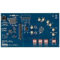
Manufacturer Part Number
AD9551/PCBZ
Description
BOARD EVAL FOR AD9951
Manufacturer
Analog Devices Inc
Datasheet
1.AD9551PCBZ.pdf
(40 pages)
Specifications of AD9551/PCBZ
Main Purpose
Timing, Clock Generator
Embedded
No
Utilized Ic / Part
AD9551
Primary Attributes
2 Inputs, 2 Outputs, VCO
Secondary Attributes
Graphical User Interface, USB Interface
Silicon Manufacturer
Analog Devices
Application Sub Type
Clock Generator
Kit Application Type
Clock & Timing
Silicon Core Number
AD9551
Kit Contents
Board
Lead Free Status / RoHS Status
Lead free / RoHS Compliant


REGISTER MAP
A bit that is labeled “aclr” is an active high, autoclearing bit. When set to a Logic 1 state, the control logic automatically returns it to
a Logic 0 state upon completion of the indicated task.
Table 22. Register Map
Addr.
(Hex)
0x00
0x04
0x05
0x0A
0x0B
0x0C
0x0D
0x0E
0x0F
0x10
0x11
0x12
0x13
0x14
0x15
0x16
0x17
0x18
Register
Name
Serial port
control
Readback
control
I/O update
Output PLL
PFD and
charge
pump
Output PLL
PFD and
charge
pump
Output PLL
PFD and
charge
pump
Output PLL
PFD and
charge
pump
VCO
control
VCO
control
VCO
control
Output PLL
control
Output PLL
control
Output PLL
control
Output PLL
control
Output PLL
control
Output PLL
control
Output PLL
control
Output PLL
control
(MSB)
Bit 7
0
Unused
Unused
Enable SPI
control of
charge
pump
current
Unused
Calibrate
VCO (aclr)
Antibacklash
FRAC[3:0] (output SDM fractional part)
control[1:0]
MOD[3:0] (output SDM modulus)
Bit 6
LSB first
Unused
Unused
Enable SPI
control of
antiback-
lash
period
CP offset
current
polarity
Enable
automatic
level
control
P
Unused
Automatic level control threshold[2:0]
1
Bit 5
Soft reset
(aclr)
Unused
Unused
CP offset current[1:0]
divider[4:0]
Output PLL PDF and charge pump current control[7:0]
VCO level control[5:0]
CP mode[1:0]
FRAC[19:12] (output SDM fractional part)
FRAC[11:4] (output SDM fractional part)
(3.5 μA granularity, ~900 μA full scale)
VCO band control[6:0]
MOD[19:12] (output SDM modulus)
MOD[11:4] (output SDM modulus)
Bit 4
1
Unused
Unused
Unused
N[7:0] (output SDM integer part)
Rev. B | Page 29 of 40
Bit 3
1
Unused
Unused
Enable CP
mode
control
Enable CP
offset
current
control
Unused
Enable SPI
control of
output
frequency
Enable
OUTPUT
PLL LOCKED
pin as test
port
Bit 2
Device reset
Unused
Unused
PFD
feedback
input edge
control
Reserved/
enable PFD
up divide-
by-2
Unused
Enable SPI
control of
VCO
calibration
Bypass
output SDM
Test mux control[1:0]
P0 divider[2:0]
Bit 1
LSB first
Unused
Unused
PFD
reference
input edge
control
Reserved/
enable PFD
down divide-
by-2
Unused
Boost VCO
supply
Unused
Disable
output SDM
(LSB)
Bit 0
Readback
control
(aclr)
Force VCO
to midpoint
frequency
Reserved/
enable
feedback
divide-by-2
lock
detector
power-
down
Enable SPI
control of
VCO band
setting
Unused
Unused
Reset
output PLL
P
0
I/O update
Output PLL
1
divider[5]
AD9551
Default
0x18
0x00
0x00
0x80
0x30
0x00
0x00
0x70
0x80
0x80
0x80
0x00
0x00
0x20
0x00
0x01
0x00
0x00
Related parts for AD9551/PCBZ
Image
Part Number
Description
Manufacturer
Datasheet
Request
R


Part Number:
Description:
±1.7g Dual-Axis IMEMS Accelerometer Evaluation Board
Manufacturer:
Analog Devices Inc
Datasheet:

Part Number:
Description:
Inertial Sensor Evaluation System
Manufacturer:
Analog Devices Inc
Datasheet:
Part Number:
Description:
Manufacturer:
Analog Devices Inc
Datasheet:
Part Number:
Description:
Manufacturer:
Analog Devices Inc
Datasheet:
Part Number:
Description:
Manufacturer:
Analog Devices Inc
Datasheet:
Part Number:
Description:
Manufacturer:
Analog Devices Inc
Datasheet:
Part Number:
Description:
Manufacturer:
Analog Devices Inc
Datasheet:
Part Number:
Description:
Manufacturer:
Analog Devices Inc
Datasheet:
Part Number:
Description:
Manufacturer:
Analog Devices Inc
Datasheet:
Part Number:
Description:
Manufacturer:
Analog Devices Inc
Datasheet:
Part Number:
Description:
Manufacturer:
Analog Devices Inc
Datasheet:
Part Number:
Description:
Manufacturer:
Analog Devices Inc
Datasheet: