C8051F410DK Silicon Laboratories Inc, C8051F410DK Datasheet - Page 10
C8051F410DK
Manufacturer Part Number
C8051F410DK
Description
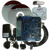
KIT DEV FOR C8051F41X
Manufacturer
Silicon Laboratories Inc
Type
MCUr
Specifications of C8051F410DK
Contents
Evaluation Board, Power Supply, USB Cables, Adapter and Documentation
Processor To Be Evaluated
C8051F41x
Interface Type
USB
Silicon Manufacturer
Silicon Labs
Core Architecture
8051
Silicon Core Number
C8051F410
Silicon Family Name
C8051F41x
Lead Free Status / RoHS Status
Contains lead / RoHS non-compliant
For Use With/related Products
Silicon Laboratories C8051F41x
Lead Free Status / Rohs Status
Lead free / RoHS Compliant
Other names
336-1314
Available stocks
Company
Part Number
Manufacturer
Quantity
Price
Company:

Part Number:
C8051F410DK
Manufacturer:
Silicon Labs
Quantity:
135


C8051F410/1/2/3
10. CIP-51 Microcontroller
11. Memory Organization and SFRs
12. Interrupt Handler
13. Prefetch Engine
14. Cyclic Redundancy Check Unit (CRC0)
15. Reset Sources
16. Flash Memory
17. External RAM
18. Port Input/Output
19. Oscillators
20. smaRTClock (Real Time Clock)
21. SMBus
22. UART0
10
Figure 9.3. Comparator Hysteresis Plot ................................................................... 85
Figure 10.1. CIP-51 Block Diagram.......................................................................... 93
Figure 11.1. Memory Map ...................................................................................... 103
Figure 14.1. CRC0 Block Diagram ......................................................................... 121
Figure 14.2. Bit Reverse Register .......................................................................... 124
Figure 15.1. Reset Sources.................................................................................... 127
Figure 15.2. Power-On and VDD Monitor Reset Timing ........................................ 128
Figure 16.1. Flash Program Memory Map.............................................................. 137
Figure 18.1. Port I/O Functional Block Diagram ..................................................... 147
Figure 18.2. Port I/O Cell Block Diagram ............................................................... 148
Figure 18.3. Crossbar Priority Decoder with No Pins Skipped ............................... 149
Figure 18.4. Crossbar Priority Decoder with Crystal Pins Skipped ........................ 150
Figure 18.5. Port 0 Input Overdrive Current Range................................................ 152
Figure 19.1. Oscillator Diagram.............................................................................. 165
Figure 19.2. 32.768 kHz External Crystal Example................................................ 169
Figure 19.3. Example Clock Multiplier Output ........................................................ 172
Figure 20.1. smaRTClock Block Diagram .............................................................. 177
Figure 21.1. SMBus Block Diagram ....................................................................... 191
Figure 21.2. Typical SMBus Configuration ............................................................. 192
Figure 21.3. SMBus Transaction ............................................................................ 193
Figure 21.4. Typical SMBus SCL Generation......................................................... 196
Figure 21.5. Typical Master Transmitter Sequence................................................ 202
Figure 21.6. Typical Master Receiver Sequence.................................................... 202
Figure 21.7. Typical Slave Receiver Sequence...................................................... 203
Figure 21.8. Typical Slave Transmitter Sequence.................................................. 204
Figure 22.1. UART0 Block Diagram ....................................................................... 207
Figure 22.2. UART0 Baud Rate Logic .................................................................... 208
Figure 22.3. UART Interconnect Diagram .............................................................. 209
Figure 22.4. 8-Bit UART Timing Diagram............................................................... 209
Figure 22.5. 9-Bit UART Timing Diagram............................................................... 210
Figure 22.6. UART Multi-Processor Mode Interconnect Diagram .......................... 211
Rev. 1.1
Related parts for C8051F410DK
Image
Part Number
Description
Manufacturer
Datasheet
Request
R

Part Number:
Description:
SMD/C°/SINGLE-ENDED OUTPUT SILICON OSCILLATOR
Manufacturer:
Silicon Laboratories Inc
Part Number:
Description:
Manufacturer:
Silicon Laboratories Inc
Datasheet:
Part Number:
Description:
N/A N/A/SI4010 AES KEYFOB DEMO WITH LCD RX
Manufacturer:
Silicon Laboratories Inc
Datasheet:
Part Number:
Description:
N/A N/A/SI4010 SIMPLIFIED KEY FOB DEMO WITH LED RX
Manufacturer:
Silicon Laboratories Inc
Datasheet:
Part Number:
Description:
N/A/-40 TO 85 OC/EZLINK MODULE; F930/4432 HIGH BAND (REV E/B1)
Manufacturer:
Silicon Laboratories Inc
Part Number:
Description:
EZLink Module; F930/4432 Low Band (rev e/B1)
Manufacturer:
Silicon Laboratories Inc
Part Number:
Description:
I°/4460 10 DBM RADIO TEST CARD 434 MHZ
Manufacturer:
Silicon Laboratories Inc
Part Number:
Description:
I°/4461 14 DBM RADIO TEST CARD 868 MHZ
Manufacturer:
Silicon Laboratories Inc
Part Number:
Description:
I°/4463 20 DBM RFSWITCH RADIO TEST CARD 460 MHZ
Manufacturer:
Silicon Laboratories Inc
Part Number:
Description:
I°/4463 20 DBM RADIO TEST CARD 868 MHZ
Manufacturer:
Silicon Laboratories Inc
Part Number:
Description:
I°/4463 27 DBM RADIO TEST CARD 868 MHZ
Manufacturer:
Silicon Laboratories Inc
Part Number:
Description:
I°/4463 SKYWORKS 30 DBM RADIO TEST CARD 915 MHZ
Manufacturer:
Silicon Laboratories Inc
Part Number:
Description:
N/A N/A/-40 TO 85 OC/4463 RFMD 30 DBM RADIO TEST CARD 915 MHZ
Manufacturer:
Silicon Laboratories Inc
Part Number:
Description:
I°/4463 20 DBM RADIO TEST CARD 169 MHZ
Manufacturer:
Silicon Laboratories Inc