C8051F410DK Silicon Laboratories Inc, C8051F410DK Datasheet - Page 174
C8051F410DK
Manufacturer Part Number
C8051F410DK
Description
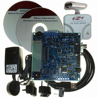
KIT DEV FOR C8051F41X
Manufacturer
Silicon Laboratories Inc
Type
MCUr
Specifications of C8051F410DK
Contents
Evaluation Board, Power Supply, USB Cables, Adapter and Documentation
Processor To Be Evaluated
C8051F41x
Interface Type
USB
Silicon Manufacturer
Silicon Labs
Core Architecture
8051
Silicon Core Number
C8051F410
Silicon Family Name
C8051F41x
Lead Free Status / RoHS Status
Contains lead / RoHS non-compliant
For Use With/related Products
Silicon Laboratories C8051F41x
Lead Free Status / Rohs Status
Lead free / RoHS Compliant
Other names
336-1314
Available stocks
Company
Part Number
Manufacturer
Quantity
Price
Company:

Part Number:
C8051F410DK
Manufacturer:
Silicon Labs
Quantity:
135


C8051F410/1/2/3
19.4. System Clock Selection
The internal oscillator requires little start-up time and may be selected as the system clock immediately fol-
lowing the OSCICN write that enables the internal oscillator. External crystals and ceramic resonators typ-
ically require a start-up time before they are settled and ready for use. The Crystal Valid Flag (XTLVLD in
register OSCXCN) is set to ‘1’ by hardware when the external oscillator is settled. To avoid reading a
false XTLVLD, in crystal mode software should delay at least 1 ms between enabling the external
oscillator and checking XTLVLD. RC and C modes typically require no startup time.
The CLKSL[1:0] bits in register CLKSEL select which oscillator source is used as the system clock.
CLKSL[1:0] must be set to 01b for the system clock to run from the external oscillator; however the exter-
nal oscillator may still clock certain peripherals (timers, PCA) when another oscillator is selected as the
system clock. The system clock may be switched on-the-fly between the internal oscillator, external oscilla-
tor, smaRTClock oscillator, and Clock Multiplier, as long as the selected clock source is enabled and has
settled.
174
Bits7–6: Unused. Read = 00b; Write = don’t care.
Bits5–4: CLKDIV1–0: Output /SYSCLK Divide Value
Bit3:
Bit2:
Bits1–0: CLKSL1–0: System Clock Select
Bit7
R
-
These bits can be used to pre-divide the /SYSCLK output before it is sent to a port pin
through the Crossbar.
00: Output will be SYSCLK.
01: Output will be SYSCLK/2.
10: Output will be SYSCLK/4.
11: Output will be SYSCLK/8.
Unused. Read = 0b; Write = don’t care.
Reserved. Read = 0b; Must write 0b.
These bits select the system clock source.
Bit6
R
-
CLKSL
00
01
10
11
SFR Definition 19.5. CLKSEL: Clock Select
R/W
Bit5
CLKDIV
R/W
Bit4
Internal Oscillator (as determined by the
IFCN bits in register OSCICN)
Rev. 1.1
smaRTClock Oscillator
Bit3
External Oscillator
R
-
Selected Clock
Clock Multiplier
Reserved
R/W
Bit2
R/W
Bit1
CLKSL
SFR Address:
R/W
Bit0
0xA9
00000000
Reset Value
Related parts for C8051F410DK
Image
Part Number
Description
Manufacturer
Datasheet
Request
R

Part Number:
Description:
SMD/C°/SINGLE-ENDED OUTPUT SILICON OSCILLATOR
Manufacturer:
Silicon Laboratories Inc
Part Number:
Description:
Manufacturer:
Silicon Laboratories Inc
Datasheet:
Part Number:
Description:
N/A N/A/SI4010 AES KEYFOB DEMO WITH LCD RX
Manufacturer:
Silicon Laboratories Inc
Datasheet:
Part Number:
Description:
N/A N/A/SI4010 SIMPLIFIED KEY FOB DEMO WITH LED RX
Manufacturer:
Silicon Laboratories Inc
Datasheet:
Part Number:
Description:
N/A/-40 TO 85 OC/EZLINK MODULE; F930/4432 HIGH BAND (REV E/B1)
Manufacturer:
Silicon Laboratories Inc
Part Number:
Description:
EZLink Module; F930/4432 Low Band (rev e/B1)
Manufacturer:
Silicon Laboratories Inc
Part Number:
Description:
I°/4460 10 DBM RADIO TEST CARD 434 MHZ
Manufacturer:
Silicon Laboratories Inc
Part Number:
Description:
I°/4461 14 DBM RADIO TEST CARD 868 MHZ
Manufacturer:
Silicon Laboratories Inc
Part Number:
Description:
I°/4463 20 DBM RFSWITCH RADIO TEST CARD 460 MHZ
Manufacturer:
Silicon Laboratories Inc
Part Number:
Description:
I°/4463 20 DBM RADIO TEST CARD 868 MHZ
Manufacturer:
Silicon Laboratories Inc
Part Number:
Description:
I°/4463 27 DBM RADIO TEST CARD 868 MHZ
Manufacturer:
Silicon Laboratories Inc
Part Number:
Description:
I°/4463 SKYWORKS 30 DBM RADIO TEST CARD 915 MHZ
Manufacturer:
Silicon Laboratories Inc
Part Number:
Description:
N/A N/A/-40 TO 85 OC/4463 RFMD 30 DBM RADIO TEST CARD 915 MHZ
Manufacturer:
Silicon Laboratories Inc
Part Number:
Description:
I°/4463 20 DBM RADIO TEST CARD 169 MHZ
Manufacturer:
Silicon Laboratories Inc