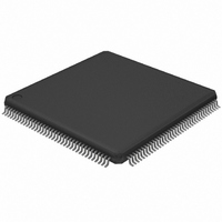
LPC2929FBD144,551 NXP Semiconductors, LPC2929FBD144,551 Datasheet - Page 16

LPC2929FBD144,551
Manufacturer Part Number
LPC2929FBD144,551
Description
IC ARM9 MCU FLASH 768K 144LQFP
Manufacturer
NXP Semiconductors
Series
LPC2900r
Datasheet
1.LPC2929FBD144551.pdf
(95 pages)
Specifications of LPC2929FBD144,551
Program Memory Type
FLASH
Program Memory Size
768KB (768K x 8)
Package / Case
144-LQFP
Core Processor
ARM9
Core Size
32-Bit
Speed
125MHz
Connectivity
CAN, EBI/EMI, I²C, LIN, SPI, UART/USART, USB
Peripherals
DMA, POR, PWM, WDT
Number Of I /o
104
Eeprom Size
16K x 8
Ram Size
56K x 8
Voltage - Supply (vcc/vdd)
1.71 V ~ 3.6 V
Data Converters
A/D 24x10b
Oscillator Type
Internal
Operating Temperature
-40°C ~ 85°C
Processor Series
LPC29
Core
ARM968E-S
Data Bus Width
16 bit, 32 bit
Data Ram Size
56 KB
Interface Type
CAN/UART/USB
Maximum Clock Frequency
125 MHz
Number Of Programmable I/os
104
Number Of Timers
6
Operating Supply Voltage
1.8 V
Maximum Operating Temperature
+ 85 C
Mounting Style
SMD/SMT
3rd Party Development Tools
MDK-ARM, RL-ARM, ULINK2, MCB2929, MCB2929U, MCB2929UME
Development Tools By Supplier
OM11026, OM11038
Minimum Operating Temperature
- 40 C
On-chip Adc
3 (8-ch x 10-bit)
Package
144LQFP
Device Core
ARM968E-S
Family Name
LPC2900
Maximum Speed
125 MHz
Lead Free Status / RoHS Status
Lead free / RoHS Compliant
For Use With
568-4786 - EXT BOARD MOTOR CONTROL LPC2900
Lead Free Status / Rohs Status
Lead free / RoHS Compliant
Other names
568-4695
935287118551
LPC2929FBD144-S
935287118551
LPC2929FBD144-S
Available stocks
Company
Part Number
Manufacturer
Quantity
Price
Company:
Part Number:
LPC2929FBD144,551
Manufacturer:
NXP Semiconductors
Quantity:
10 000
NXP Semiconductors
LPC2926_27_29
Product data sheet
6.6.3.1 ETM/ETB
6.6.4 Power supply pins
6.7.1 Clock architecture
6.7 Clocking strategy
The ETM provides real-time trace capability for deeply embedded processor cores. It
outputs information about processor execution to a trace buffer. A software debugger
allows configuration of the ETM using a JTAG interface and displays the trace information
that has been captured in a format that a user can easily understand. The ETB stores
trace data produced by the ETM.
The ETM/ETB module has the following features:
Table 6
Table 6.
The LPC2926/2927/2929 contains several different internal clock areas. Peripherals like
Timers, SPI, UART, CAN and LIN have their own individual clock sources called base
clocks. All base clocks are generated by the Clock Generator Unit (CGU0). They may be
unrelated in frequency and phase and can have different clock sources within the CGU.
The system clock for the CPU and AHB Bus infrastructure has its own base clock. This
means most peripherals are clocked independently from the system clock. See
for an overview of the clock areas within the device.
Within each clock area there may be multiple branch clocks, which offers very flexible
control for power-management purposes. All branch clocks are outputs of the Power
Management Unit (PMU) and can be controlled independently. Branch clocks derived
from the same base clock are synchronous in frequency and phase. See
more details of clock and power control within the device.
Symbol
V
V
V
V
V
V
V
V
V
•
•
•
•
•
DD(CORE)
SS(CORE)
DD(IO)
SS(IO)
DD(OSC_PLL)
SS(OSC)
SS(PLL)
DDA(ADC3V3)
DDA(ADC5V0)
Closely tracks the instructions that the ARM core is executing.
On-chip trace data storage (ETB).
All registers are programmed through JTAG interface.
Does not consume power when trace is not being used.
THUMB/Java instruction set support.
shows the power supply pins.
Power supply pins
Description
digital core supply 1.8 V
digital core ground (digital core, ADC0/1/2)
I/O pins supply 3.3 V
I/O pins ground
oscillator and PLL supply
oscillator ground
PLL ground
ADC1 and ADC2 3.3 V supply
ADC0 5.0 V supply
All information provided in this document is subject to legal disclaimers.
Rev. 5 — 28 September 2010
ARM9 microcontroller with CAN, LIN, and USB
LPC2926/2927/2929
© NXP B.V. 2010. All rights reserved.
Section 6.16
Figure 4
16 of 95
for


