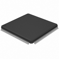
LPC2929FBD144,551 NXP Semiconductors, LPC2929FBD144,551 Datasheet - Page 19

LPC2929FBD144,551
Manufacturer Part Number
LPC2929FBD144,551
Description
IC ARM9 MCU FLASH 768K 144LQFP
Manufacturer
NXP Semiconductors
Series
LPC2900r
Datasheet
1.LPC2929FBD144551.pdf
(95 pages)
Specifications of LPC2929FBD144,551
Program Memory Type
FLASH
Program Memory Size
768KB (768K x 8)
Package / Case
144-LQFP
Core Processor
ARM9
Core Size
32-Bit
Speed
125MHz
Connectivity
CAN, EBI/EMI, I²C, LIN, SPI, UART/USART, USB
Peripherals
DMA, POR, PWM, WDT
Number Of I /o
104
Eeprom Size
16K x 8
Ram Size
56K x 8
Voltage - Supply (vcc/vdd)
1.71 V ~ 3.6 V
Data Converters
A/D 24x10b
Oscillator Type
Internal
Operating Temperature
-40°C ~ 85°C
Processor Series
LPC29
Core
ARM968E-S
Data Bus Width
16 bit, 32 bit
Data Ram Size
56 KB
Interface Type
CAN/UART/USB
Maximum Clock Frequency
125 MHz
Number Of Programmable I/os
104
Number Of Timers
6
Operating Supply Voltage
1.8 V
Maximum Operating Temperature
+ 85 C
Mounting Style
SMD/SMT
3rd Party Development Tools
MDK-ARM, RL-ARM, ULINK2, MCB2929, MCB2929U, MCB2929UME
Development Tools By Supplier
OM11026, OM11038
Minimum Operating Temperature
- 40 C
On-chip Adc
3 (8-ch x 10-bit)
Package
144LQFP
Device Core
ARM968E-S
Family Name
LPC2900
Maximum Speed
125 MHz
Lead Free Status / RoHS Status
Lead free / RoHS Compliant
For Use With
568-4786 - EXT BOARD MOTOR CONTROL LPC2900
Lead Free Status / Rohs Status
Lead free / RoHS Compliant
Other names
568-4695
935287118551
LPC2929FBD144-S
935287118551
LPC2929FBD144-S
Available stocks
Company
Part Number
Manufacturer
Quantity
Price
Company:
Part Number:
LPC2929FBD144,551
Manufacturer:
NXP Semiconductors
Quantity:
10 000
NXP Semiconductors
LPC2926_27_29
Product data sheet
Table 7.
[1]
[2]
[3]
[4]
Table 8.
Base clock
BASE_MSCSS_CLK
BASE_UART_CLK
BASE_ICLK0_CLK
BASE_SPI_CLK
BASE_TMR_CLK
BASE_ADC_CLK
reserved
BASE_ICLK1_CLK
Base clock
BASE_OUT_CLK
BASE_USB_CLK
BASE_USB_I2C_CLK
This clock is always on (cannot be switched off for system safety reasons).
In the peripheral subsystem parts of the timers, watchdog timer, SPI and UART have their own clock
source. See
The clock should remain activated when system wake-up on timer or UART is required.
In the Power Clock and Reset Control subsystem parts of the CGU, RGU, and PMU have their own clock
source. See
CGU0 base clock and branch clock overview
CGU1 base clock and branch clock overview
Section 6.13
Section 6.16
All information provided in this document is subject to legal disclaimers.
Rev. 5 — 28 September 2010
for details.
for details.
Branch clock name
CLK_MSCSS_APB
CLK_MSCSS_MTMR0
CLK_MSCSS_MTMR1
CLK_MSCSS_PWM0
CLK_MSCSS_PWM1
CLK_MSCSS_PWM2
CLK_MSCSS_PWM3
CLK_MSCSS_ADC0_APB APB side of ADC 0
CLK_MSCSS_ADC1_APB APB side of ADC 1
CLK_MSCSS_ADC2_APB APB side of ADC 2
CLK_MSCSS_QEI
CLK_UART0
CLK_UART1
-
CLK_SPI0
CLK_SPI1
CLK_SPI2
CLK_TMR0
CLK_TMR1
CLK_TMR2
CLK_TMR3
CLK_ADC0
CLK_ADC1
CLK_ADC2
-
-
Branch clock name
CLK_OUT_CLK
CLK_USB_CLK
CLK_USB_I2C_CLK
ARM9 microcontroller with CAN, LIN, and USB
LPC2926/2927/2929
Parts of the device clocked
by this branch clock
APB side of the MSCSS
Timer 0 in the MSCSS
Timer 1 in the MSCSS
PWM 0
PWM 1
PWM 2
PWM 3
Quadrature encoder
CGU1 input clock
SPI 0 interface clock
SPI 1 interface clock
SPI 2 interface clock
Timer 0 clock for counter part
Timer 1 clock for counter part
Timer 2 clock for counter part
Timer 3 clock for counter part
sample result
Control of ADC 1, capture
sample result
Control of ADC 2, capture
sample result
-
CGU1 input clock
Parts of the device clocked
by this branch clock
clock out pin
USB OTG I2C clock
UART 0 interface clock
UART 1 interface clock
Control of ADC 0, capture
USB clock
…continued
© NXP B.V. 2010. All rights reserved.
Remark
Remark
19 of 95


