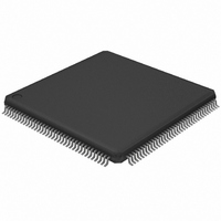
LPC2929FBD144,551 NXP Semiconductors, LPC2929FBD144,551 Datasheet - Page 66

LPC2929FBD144,551
Manufacturer Part Number
LPC2929FBD144,551
Description
IC ARM9 MCU FLASH 768K 144LQFP
Manufacturer
NXP Semiconductors
Series
LPC2900r
Datasheet
1.LPC2929FBD144551.pdf
(95 pages)
Specifications of LPC2929FBD144,551
Program Memory Type
FLASH
Program Memory Size
768KB (768K x 8)
Package / Case
144-LQFP
Core Processor
ARM9
Core Size
32-Bit
Speed
125MHz
Connectivity
CAN, EBI/EMI, I²C, LIN, SPI, UART/USART, USB
Peripherals
DMA, POR, PWM, WDT
Number Of I /o
104
Eeprom Size
16K x 8
Ram Size
56K x 8
Voltage - Supply (vcc/vdd)
1.71 V ~ 3.6 V
Data Converters
A/D 24x10b
Oscillator Type
Internal
Operating Temperature
-40°C ~ 85°C
Processor Series
LPC29
Core
ARM968E-S
Data Bus Width
16 bit, 32 bit
Data Ram Size
56 KB
Interface Type
CAN/UART/USB
Maximum Clock Frequency
125 MHz
Number Of Programmable I/os
104
Number Of Timers
6
Operating Supply Voltage
1.8 V
Maximum Operating Temperature
+ 85 C
Mounting Style
SMD/SMT
3rd Party Development Tools
MDK-ARM, RL-ARM, ULINK2, MCB2929, MCB2929U, MCB2929UME
Development Tools By Supplier
OM11026, OM11038
Minimum Operating Temperature
- 40 C
On-chip Adc
3 (8-ch x 10-bit)
Package
144LQFP
Device Core
ARM968E-S
Family Name
LPC2900
Maximum Speed
125 MHz
Lead Free Status / RoHS Status
Lead free / RoHS Compliant
For Use With
568-4786 - EXT BOARD MOTOR CONTROL LPC2900
Lead Free Status / Rohs Status
Lead free / RoHS Compliant
Other names
568-4695
935287118551
LPC2929FBD144-S
935287118551
LPC2929FBD144-S
Available stocks
Company
Part Number
Manufacturer
Quantity
Price
Company:
Part Number:
LPC2929FBD144,551
Manufacturer:
NXP Semiconductors
Quantity:
10 000
NXP Semiconductors
Table 35.
V
[1]
[2]
[3]
[4]
[5]
[6]
[7]
[8]
LPC2926_27_29
Product data sheet
Symbol
V
V
V
Z
C
E
E
E
E
E
R
FSR
DDA(ADC3V3)
Fig 16. Suggested ADC interface - LPC2926/2927/2929 ADC1/2 IN[y] pin
i
VREFN
VREFP
IA
D
L(adj)
O
G
T
ia
vsi
Conditions: V
The ADC is monotonic, there are no missing codes.
The differential linearity error (E
The integral non-linearity (E
appropriate adjustment of gain and offset errors. See
The offset error (E
ideal curve. See
The gain error (E
error, and the straight line which fits the ideal transfer curve. See
The absolute error (E
ADC and the ideal transfer curve. See
See
Figure
ADC static characteristics
= 3.0 V to 3.6 V; T
Parameter
voltage on pin VREFN
voltage on pin VREFP
analog input voltage
input impedance
analog input capacitance
differential linearity error
integral non-linearity
offset error
gain error
absolute error
voltage source interface
resistance
full scale range
16.
SS(IO)
Figure
G
O
) is the relative difference in percent between the straight line fitting the actual transfer curve after removing offset
= 0 V, V
) is the absolute difference between the straight line which fits the actual curve and the straight line which fits the
T
) is the maximum difference between the center of the steps of the actual transfer curve of the non-calibrated
17.
DDA(ADC3V3)
L(adj)
ADC IN[y]
amb
D
) is the peak difference between the center of the steps of the actual and the ideal transfer curve after
) is the difference between the actual step width and the ideal step width. See
=
SAMPLE
−
40
Figure
= 3.3 V.
°
All information provided in this document is subject to legal disclaimers.
C to +85
Conditions
for 3.3 V ADC1/2
between V
V
between V
V
for ADC0/1/2
for ADC0/1/2
for ADC0/1/2
for ADC0/1/2
for ADC0/1/2
for ADC0/1/2
for ADC0/1/2
for ADC0/1/2
VREFP
DDA(ADC5V0)
17.
LPC2XXX
Rev. 5 — 28 September 2010
V
3 pF
SS(IO),
°
Figure
C unless otherwise specified; ADC frequency 4.5 MHz.
VREFN
VREFN
20 kΩ
V
SS(CORE)
17.
and
and
Figure
5 pF
17.
ARM9 microcontroller with CAN, LIN, and USB
[1][2][3]
[1][4]
[1][5]
[1][6]
[1][7]
[8]
ADC IN[y]
2
Min
0
V
V
4.4
13.7
-
-
-
-
-
-
-
LPC2926/2927/2929
VREFN
VREFN
R vsi
+ 2 -
Typ
-
-
-
-
-
-
-
-
-
-
-
-
002aae280
V EXT
Max
V
V
V
-
23.6
1
±1
±2
±3
±0.5
±4
40
10
VREFP
DDA(ADC3V3)
VREFP
Figure
© NXP B.V. 2010. All rights reserved.
− 2
17.
Unit
V
V
V
kΩ
kΩ
pF
LSB
LSB
LSB
%
LSB
kΩ
bit
66 of 95


