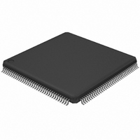
LPC2929FBD144,551 NXP Semiconductors, LPC2929FBD144,551 Datasheet - Page 35

LPC2929FBD144,551
Manufacturer Part Number
LPC2929FBD144,551
Description
IC ARM9 MCU FLASH 768K 144LQFP
Manufacturer
NXP Semiconductors
Series
LPC2900r
Datasheet
1.LPC2929FBD144551.pdf
(95 pages)
Specifications of LPC2929FBD144,551
Program Memory Type
FLASH
Program Memory Size
768KB (768K x 8)
Package / Case
144-LQFP
Core Processor
ARM9
Core Size
32-Bit
Speed
125MHz
Connectivity
CAN, EBI/EMI, I²C, LIN, SPI, UART/USART, USB
Peripherals
DMA, POR, PWM, WDT
Number Of I /o
104
Eeprom Size
16K x 8
Ram Size
56K x 8
Voltage - Supply (vcc/vdd)
1.71 V ~ 3.6 V
Data Converters
A/D 24x10b
Oscillator Type
Internal
Operating Temperature
-40°C ~ 85°C
Processor Series
LPC29
Core
ARM968E-S
Data Bus Width
16 bit, 32 bit
Data Ram Size
56 KB
Interface Type
CAN/UART/USB
Maximum Clock Frequency
125 MHz
Number Of Programmable I/os
104
Number Of Timers
6
Operating Supply Voltage
1.8 V
Maximum Operating Temperature
+ 85 C
Mounting Style
SMD/SMT
3rd Party Development Tools
MDK-ARM, RL-ARM, ULINK2, MCB2929, MCB2929U, MCB2929UME
Development Tools By Supplier
OM11026, OM11038
Minimum Operating Temperature
- 40 C
On-chip Adc
3 (8-ch x 10-bit)
Package
144LQFP
Device Core
ARM968E-S
Family Name
LPC2900
Maximum Speed
125 MHz
Lead Free Status / RoHS Status
Lead free / RoHS Compliant
For Use With
568-4786 - EXT BOARD MOTOR CONTROL LPC2900
Lead Free Status / Rohs Status
Lead free / RoHS Compliant
Other names
568-4695
935287118551
LPC2929FBD144-S
935287118551
LPC2929FBD144-S
Available stocks
Company
Part Number
Manufacturer
Quantity
Price
Company:
Part Number:
LPC2929FBD144,551
Manufacturer:
NXP Semiconductors
Quantity:
10 000
NXP Semiconductors
LPC2926_27_29
Product data sheet
6.13.5.3 Clock description
6.13.6.1 Functional description
6.13.6.2 Pin description
6.13.6 General-purpose I/O
Table 18.
[1]
[2]
The SPI modules are clocked by two different clocks; CLK_SYS_PESS and CLK_SPIx
(x = 0, 1, 2), see
power management. The frequency of all clocks CLK_SPIx is identical as they are derived
from the same base clock BASE_CLK_SPI. The register interface towards the system bus
is clocked by CLK_SYS_PESS. The serial-clock rate divisor is clocked by CLK_SPIx.
The SPI clock frequency can be controlled by the CGU. In master mode the SPI clock
frequency (CLK_SPIx) must be set to at least twice the SPI serial clock rate on the
interface. In slave mode CLK_SPIx must be set to four times the SPI serial clock rate on
the interface.
The LPC2926/2927/2929 contains four general-purpose I/O ports located at different
peripheral base addresses. In the 144-pin package all four ports are available. All I/O pins
are bidirectional, and the direction can be programmed individually. The I/O pad behavior
depends on the configuration programmed in the port function-select registers.
The key features are:
The general-purpose I/O provides individual control over each bidirectional port pin. There
are two registers to control I/O direction and output level. The inputs are synchronized to
achieve stable read-levels.
To generate an open-drain output, set the bit in the output register to the desired value.
Use the direction register to control the signal. When set to output, the output driver
actively drives the value on the output: when set to input the signal floats and can be
pulled up internally or externally.
The five GPIO ports in the LPC2926/2927/2929 have the pins listed below. The GPIO pins
are combined with other functions on the port pins of the LPC2926/2927/2929.
shows the GPIO pins.
Symbol
SPIx SCK
SPIx SDI
SPIx SDO
•
•
•
•
Direction of SPIx SCS and SPIx SCK pins depends on master or slave mode. These pins are output in
master mode, input in slave mode.
In slave mode there is only one chip select input pin, SPIx SCS0. The other chip selects have no function in
slave mode.
General-purpose parallel inputs and outputs
Direction control of individual bits
Synchronized input sampling for stable input-data values
All I/O defaults to input at reset to avoid any possible bus conflicts
SPI pins
SCKx
SDIx
SDOx
Pin name
All information provided in this document is subject to legal disclaimers.
Section
…continued
Rev. 5 — 28 September 2010
6.7.2. Note that each SPI has its own CLK_SPIx branch clock for
IN
OUT
Direction
IN/OUT
ARM9 microcontroller with CAN, LIN, and USB
SPIx data input
SPIx data output
Description
SPIx clock
LPC2926/2927/2929
[1]
© NXP B.V. 2010. All rights reserved.
Table 19
35 of 95


