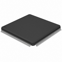
LPC2929FBD144,551 NXP Semiconductors, LPC2929FBD144,551 Datasheet - Page 53

LPC2929FBD144,551
Manufacturer Part Number
LPC2929FBD144,551
Description
IC ARM9 MCU FLASH 768K 144LQFP
Manufacturer
NXP Semiconductors
Series
LPC2900r
Datasheet
1.LPC2929FBD144551.pdf
(95 pages)
Specifications of LPC2929FBD144,551
Program Memory Type
FLASH
Program Memory Size
768KB (768K x 8)
Package / Case
144-LQFP
Core Processor
ARM9
Core Size
32-Bit
Speed
125MHz
Connectivity
CAN, EBI/EMI, I²C, LIN, SPI, UART/USART, USB
Peripherals
DMA, POR, PWM, WDT
Number Of I /o
104
Eeprom Size
16K x 8
Ram Size
56K x 8
Voltage - Supply (vcc/vdd)
1.71 V ~ 3.6 V
Data Converters
A/D 24x10b
Oscillator Type
Internal
Operating Temperature
-40°C ~ 85°C
Processor Series
LPC29
Core
ARM968E-S
Data Bus Width
16 bit, 32 bit
Data Ram Size
56 KB
Interface Type
CAN/UART/USB
Maximum Clock Frequency
125 MHz
Number Of Programmable I/os
104
Number Of Timers
6
Operating Supply Voltage
1.8 V
Maximum Operating Temperature
+ 85 C
Mounting Style
SMD/SMT
3rd Party Development Tools
MDK-ARM, RL-ARM, ULINK2, MCB2929, MCB2929U, MCB2929UME
Development Tools By Supplier
OM11026, OM11038
Minimum Operating Temperature
- 40 C
On-chip Adc
3 (8-ch x 10-bit)
Package
144LQFP
Device Core
ARM968E-S
Family Name
LPC2900
Maximum Speed
125 MHz
Lead Free Status / RoHS Status
Lead free / RoHS Compliant
For Use With
568-4786 - EXT BOARD MOTOR CONTROL LPC2900
Lead Free Status / Rohs Status
Lead free / RoHS Compliant
Other names
568-4695
935287118551
LPC2929FBD144-S
935287118551
LPC2929FBD144-S
Available stocks
Company
Part Number
Manufacturer
Quantity
Price
Company:
Part Number:
LPC2929FBD144,551
Manufacturer:
NXP Semiconductors
Quantity:
10 000
NXP Semiconductors
2.
LPC2926_27_29
Product data sheet
Generation of the main clock is restricted by the frequency range of the PLL clock input. See
6.16.2.2 PLL functional description
generator. The RDET register keeps track of which clocks are active and inactive, and the
appropriate ‘CLK_SEL’ values are masked and unmasked accordingly. Each clock
detector can also generate interrupts at clock activation and deactivation so that the
system can be notified of a change in internal clock status.
Clock detection is done using a counter running at the BASE_PCR_CLK frequency. If no
positive clock edge occurs before the counter has 32 cycles of BASE_PCR_CLK the clock
is assumed to be inactive. As BASE_PCR_CLK is slower than any of the clocks to be
detected, normally only one BASE_PCR_CLK cycle is needed to detect activity. After
reset all clocks are assumed to be ‘non-present’, so the RDET status register will be
correct only after 32 BASE_PCR_CLK cycles.
Note that this mechanism cannot protect against a currently-selected clock going from
active to inactive state. Therefore an inactive clock may still be sent to the system under
special circumstances, although an interrupt can still be generated to notify the system.
Glitch-Free Switching:
switched glitch-free, both at the output generator stage and also at secondary source
generators.
In the case of the PLL the clock will be stopped and held low for long enough to allow the
PLL to stabilize and lock before being re-enabled. For all non-PLL Generators the switch
will occur as quickly as possible, although there will always be a period when the clock is
held low due to synchronization requirements.
If the current clock is high and does not go low within 32 cycles of BASE_PCR_CLK it is
assumed to be inactive and is asynchronously forced low. This prevents deadlocks on the
interface.
A block diagram of the PLL is shown in
analog section. This block compares the phase and frequency of the inputs and generates
the main clock
divider to create the output clock, or sent directly to the output. The main output clock is
then divided by M by the programmable feedback divider to generate the feedback clock.
The output signal of the analog section is also monitored by the lock detector to signal
when the PLL has locked onto the input clock.
2
. These clocks are either divided by 2 × P by the programmable post
All information provided in this document is subject to legal disclaimers.
Rev. 5 — 28 September 2010
Provisions are included in the CGU to allow clocks to be
ARM9 microcontroller with CAN, LIN, and USB
Figure
14. The input clock is fed directly to the
LPC2926/2927/2929
Table
36, Dynamic characteristics.
© NXP B.V. 2010. All rights reserved.
53 of 95


