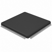
LPC2929FBD144,551 NXP Semiconductors, LPC2929FBD144,551 Datasheet - Page 65

LPC2929FBD144,551
Manufacturer Part Number
LPC2929FBD144,551
Description
IC ARM9 MCU FLASH 768K 144LQFP
Manufacturer
NXP Semiconductors
Series
LPC2900r
Datasheet
1.LPC2929FBD144551.pdf
(95 pages)
Specifications of LPC2929FBD144,551
Program Memory Type
FLASH
Program Memory Size
768KB (768K x 8)
Package / Case
144-LQFP
Core Processor
ARM9
Core Size
32-Bit
Speed
125MHz
Connectivity
CAN, EBI/EMI, I²C, LIN, SPI, UART/USART, USB
Peripherals
DMA, POR, PWM, WDT
Number Of I /o
104
Eeprom Size
16K x 8
Ram Size
56K x 8
Voltage - Supply (vcc/vdd)
1.71 V ~ 3.6 V
Data Converters
A/D 24x10b
Oscillator Type
Internal
Operating Temperature
-40°C ~ 85°C
Processor Series
LPC29
Core
ARM968E-S
Data Bus Width
16 bit, 32 bit
Data Ram Size
56 KB
Interface Type
CAN/UART/USB
Maximum Clock Frequency
125 MHz
Number Of Programmable I/os
104
Number Of Timers
6
Operating Supply Voltage
1.8 V
Maximum Operating Temperature
+ 85 C
Mounting Style
SMD/SMT
3rd Party Development Tools
MDK-ARM, RL-ARM, ULINK2, MCB2929, MCB2929U, MCB2929UME
Development Tools By Supplier
OM11026, OM11038
Minimum Operating Temperature
- 40 C
On-chip Adc
3 (8-ch x 10-bit)
Package
144LQFP
Device Core
ARM968E-S
Family Name
LPC2900
Maximum Speed
125 MHz
Lead Free Status / RoHS Status
Lead free / RoHS Compliant
For Use With
568-4786 - EXT BOARD MOTOR CONTROL LPC2900
Lead Free Status / Rohs Status
Lead free / RoHS Compliant
Other names
568-4695
935287118551
LPC2929FBD144-S
935287118551
LPC2929FBD144-S
Available stocks
Company
Part Number
Manufacturer
Quantity
Price
Company:
Part Number:
LPC2929FBD144,551
Manufacturer:
NXP Semiconductors
Quantity:
10 000
NXP Semiconductors
Table 34.
V
T
specified.
[1]
[2]
[3]
[4]
[5]
[6]
[7]
[8]
[9]
[10] The power-up reset has a time filter: V
LPC2926_27_29
Product data sheet
Symbol
I
I
I
Oscillator
V
R
C
Power-up reset
V
V
V
OL
OHS
OLS
vj
DD(CORE)
XIN_OSC
trip(high)
trip(low)
trip(dif)
s(xtal)
i
=
All parameters are guaranteed over the virtual junction temperature range by design. Pre-testing is performed at T
level. Cased products are tested at T
the specified temperature and power-supply voltage range.
Leakage current is exponential to temperature; worst-case value is at 85 °C T
V
V
Not 5 V-tolerant when pull-up is on.
For I/O Port 0, the maximum input voltage is defined by V
For Port 0, pin 0 to pin 15 add maximum 1.5 pF for input capacitance to ADC. For Port 0, pin 16 to pin 31 add maximum 1.0 pF for input
capacitance to ADC.
C
This parameter is not part of production testing or final testing, hence only a typical value is stated. Maximum and minimum values are
based on simulation results.
V
−
DDA(ADC3V3)
DDA(ADC5V0)
trip(low)
xtal
40
is crystal load capacitance and C
°
[1]
C to +85
= V
for 11 μs before internal reset is asserted.
Static characteristics
DD(OSC_PLL)
Parameter
LOW-level output current
HIGH-level short-circuit
output current
LOW-level short-circuit
output current
voltage on pin XIN_OSC
crystal series resistance
input capacitance
high trip level voltage
low trip level voltage
difference between high
and low trip level voltage
must correlate with V
must correlate with V
°
C; all voltages are measured with respect to ground; positive currents flow into the IC; unless otherwise
; V
DD(IO)
= 2.7 V to 3.6 V; V
…continued
DDA(ADC5V0)
DDA(ADC3V3)
amb
ext
DD(CORE)
= 25 °C (final testing). Both pre-testing and final testing use correlated test conditions to cover
are the two external load capacitors.
All information provided in this document is subject to legal disclaimers.
Conditions
at V
33 Ω external series
resistor
at V
external series resistor
drive high; pad
connected to ground
drive high; pad
connected to V
f
f
of XIN_OSC
osc
osc
: V
: V
C
C
C
C
C
C
must be above V
OL
= 10 MHz to 15 MHz
xtal
ext
xtal
ext
= 15 MHz to 20 MHz
xtal
ext
OL
DDA(ADC3V3)
DDA(ADC5V0)
Rev. 5 — 28 September 2010
= 0.3 V; with 33 Ω
= 18 pF
= 39 pF
= 18 pF
= 0.3 V; without
= 10 pF;
= 20 pF;
= 10 pF;
DDA(ADC3V3)
I(ADC)
DD(IO)
= V
= V
.
DDA(ADC5V0)
DDA(ADC3V3)
trip(high)
= 3.0 V to 3.6 V; V
for 2 μs before reset is de-asserted; V
ARM9 microcontroller with CAN, LIN, and USB
[10]
[10]
[10]
/ 1.5.
× 1.5.
[8]
[8]
[9]
vj
. All clocks off. Analog modules and flash powered down.
Min
26.7
5.0
-
-
0
-
-
-
-
1.1
1.0
50
LPC2926/2927/2929
DDA(ADC5V0)
Typ
-
-
-
-
-
-
-
-
1.4
1.3
120
= 3.0 V to 5.5 V;
1.8
Max
57.2
5.5
90.0
95.1
160
60
80
2
1.6
1.5
180
DD(CORE)
© NXP B.V. 2010. All rights reserved.
amb
= 85 °C on wafer
must be below
65 of 95
Unit
mA
mA
mA
mA
V
Ω
Ω
Ω
pF
V
V
mV


