MC9S08DV32ACLF Freescale Semiconductor, MC9S08DV32ACLF Datasheet - Page 13
MC9S08DV32ACLF
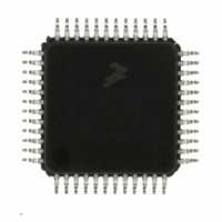
Manufacturer Part Number
MC9S08DV32ACLF
Description
IC MCU 32K FLASH 2K RAM 48-LQFP
Manufacturer
Freescale Semiconductor
Series
HCS08r
Specifications of MC9S08DV32ACLF
Core Processor
HCS08
Core Size
8-Bit
Speed
40MHz
Connectivity
CAN, I²C, LIN, SCI, SPI
Peripherals
LVD, POR, PWM, WDT
Number Of I /o
39
Program Memory Size
32KB (32K x 8)
Program Memory Type
FLASH
Ram Size
2K x 8
Voltage - Supply (vcc/vdd)
2.7 V ~ 5.5 V
Data Converters
A/D 16x12b
Oscillator Type
External
Operating Temperature
-40°C ~ 85°C
Package / Case
48-LQFP
Processor Series
S08DV
Core
HCS08
Data Bus Width
8 bit
Data Ram Size
2 KB
Interface Type
CAN, I2C, SCI, SPI
Number Of Programmable I/os
26
Operating Supply Voltage
5.5 V
Mounting Style
SMD/SMT
3rd Party Development Tools
EWS08
Development Tools By Supplier
DEMO9S08DZ60
On-chip Adc
12 bit, 10 channel
Controller Family/series
HCS08
No. Of I/o's
39
Ram Memory Size
2KB
Cpu Speed
40MHz
No. Of Timers
2
Digital Ic Case Style
LQFP
Rohs Compliant
Yes
Lead Free Status / RoHS Status
Lead free / RoHS Compliant
Eeprom Size
-
Lead Free Status / Rohs Status
Lead free / RoHS Compliant
Available stocks
Company
Part Number
Manufacturer
Quantity
Price

Company:
Part Number:
MC9S08DV32ACLF
Manufacturer:
Freescale Semiconductor
Quantity:
10 000


Section Number
10.2 External Signal Description ...........................................................................................................176
10.3 Register Definition .........................................................................................................................177
10.4 Functional Description ...................................................................................................................185
10.5 Initialization Information ...............................................................................................................191
10.6 Application Information.................................................................................................................193
11.1 Introduction ....................................................................................................................................197
11.2 External Signal Description ...........................................................................................................200
11.3 Register Definition .........................................................................................................................200
Freescale Semiconductor
10.2.1 Analog Power (V
10.2.2 Analog Ground (V
10.2.3 Voltage Reference High (V
10.2.4 Voltage Reference Low (V
10.2.5 Analog Channel Inputs (ADx) ........................................................................................177
10.3.1 Status and Control Register 1 (ADCSC1) ......................................................................177
10.3.2 Status and Control Register 2 (ADCSC2) ......................................................................179
10.3.3 Data Result High Register (ADCRH) .............................................................................179
10.3.4 Data Result Low Register (ADCRL) ..............................................................................180
10.3.5 Compare Value High Register (ADCCVH) ....................................................................180
10.3.6 Compare Value Low Register (ADCCVL) .....................................................................181
10.3.7 Configuration Register (ADCCFG) ................................................................................181
10.3.8 Pin Control 1 Register (APCTL1) ..................................................................................182
10.3.9 Pin Control 2 Register (APCTL2) ..................................................................................183
10.3.10Pin Control 3 Register (APCTL3) ..................................................................................184
10.4.1 Clock Select and Divide Control ....................................................................................186
10.4.2 Input Select and Pin Control ...........................................................................................186
10.4.3 Hardware Trigger ............................................................................................................186
10.4.4 Conversion Control .........................................................................................................186
10.4.5 Automatic Compare Function .........................................................................................189
10.4.6 MCU Wait Mode Operation ............................................................................................189
10.4.7 MCU Stop3 Mode Operation ..........................................................................................190
10.4.8 MCU Stop2 Mode Operation ..........................................................................................190
10.5.1 ADC Module Initialization Example .............................................................................191
10.6.1 External Pins and Routing ..............................................................................................193
10.6.2 Sources of Error ..............................................................................................................194
11.1.1 Features ...........................................................................................................................199
11.1.2 Modes of Operation ........................................................................................................199
11.1.3 Block Diagram ................................................................................................................200
11.2.1 SCL — Serial Clock Line ...............................................................................................200
11.2.2 SDA — Serial Data Line ................................................................................................200
Inter-Integrated Circuit (S08IICV2)
DDAD
SSAD
MC9S08DV60 Series Data Sheet, Rev 3
) ..................................................................................................177
) .................................................................................................177
REFL
REFH
Chapter 11
Subject to Change
) .....................................................................................177
) ...................................................................................177
Title
Page
13
Related parts for MC9S08DV32ACLF
Image
Part Number
Description
Manufacturer
Datasheet
Request
R

Part Number:
Description:
Manufacturer:
Freescale Semiconductor, Inc
Datasheet:
Part Number:
Description:
Manufacturer:
Freescale Semiconductor, Inc
Datasheet:
Part Number:
Description:
Manufacturer:
Freescale Semiconductor, Inc
Datasheet:
Part Number:
Description:
Manufacturer:
Freescale Semiconductor, Inc
Datasheet:
Part Number:
Description:
Manufacturer:
Freescale Semiconductor, Inc
Datasheet:
Part Number:
Description:
Manufacturer:
Freescale Semiconductor, Inc
Datasheet:
Part Number:
Description:
Manufacturer:
Freescale Semiconductor, Inc
Datasheet:
Part Number:
Description:
Manufacturer:
Freescale Semiconductor, Inc
Datasheet:
Part Number:
Description:
Manufacturer:
Freescale Semiconductor, Inc
Datasheet:
Part Number:
Description:
Manufacturer:
Freescale Semiconductor, Inc
Datasheet:
Part Number:
Description:
Manufacturer:
Freescale Semiconductor, Inc
Datasheet:
Part Number:
Description:
Manufacturer:
Freescale Semiconductor, Inc
Datasheet:
Part Number:
Description:
Manufacturer:
Freescale Semiconductor, Inc
Datasheet:
Part Number:
Description:
Manufacturer:
Freescale Semiconductor, Inc
Datasheet:
Part Number:
Description:
Manufacturer:
Freescale Semiconductor, Inc
Datasheet: