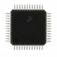
MC9S08DV32ACLF Freescale Semiconductor, MC9S08DV32ACLF Datasheet - Page 215

MC9S08DV32ACLF
Manufacturer Part Number
MC9S08DV32ACLF
Description
IC MCU 32K FLASH 2K RAM 48-LQFP
Manufacturer
Freescale Semiconductor
Series
HCS08r
Specifications of MC9S08DV32ACLF
Core Processor
HCS08
Core Size
8-Bit
Speed
40MHz
Connectivity
CAN, I²C, LIN, SCI, SPI
Peripherals
LVD, POR, PWM, WDT
Number Of I /o
39
Program Memory Size
32KB (32K x 8)
Program Memory Type
FLASH
Ram Size
2K x 8
Voltage - Supply (vcc/vdd)
2.7 V ~ 5.5 V
Data Converters
A/D 16x12b
Oscillator Type
External
Operating Temperature
-40°C ~ 85°C
Package / Case
48-LQFP
Processor Series
S08DV
Core
HCS08
Data Bus Width
8 bit
Data Ram Size
2 KB
Interface Type
CAN, I2C, SCI, SPI
Number Of Programmable I/os
26
Operating Supply Voltage
5.5 V
Mounting Style
SMD/SMT
3rd Party Development Tools
EWS08
Development Tools By Supplier
DEMO9S08DZ60
On-chip Adc
12 bit, 10 channel
Controller Family/series
HCS08
No. Of I/o's
39
Ram Memory Size
2KB
Cpu Speed
40MHz
No. Of Timers
2
Digital Ic Case Style
LQFP
Rohs Compliant
Yes
Lead Free Status / RoHS Status
Lead free / RoHS Compliant
Eeprom Size
-
Lead Free Status / Rohs Status
Lead free / RoHS Compliant
Available stocks
Company
Part Number
Manufacturer
Quantity
Price
Company:
Part Number:
MC9S08DV32ACLF
Manufacturer:
Freescale Semiconductor
Quantity:
10 000
- Current page: 215 of 414
- Download datasheet (5Mb)
NOTES:
1. If general call is enabled, a check must be done to determine whether the received address was a general call address (0x00). If the received address was a
2. When 10-bit addressing is used to address a slave, the slave sees an interrupt following the first byte of the extended address. User software must ensure that for
Freescale Semiconductor
general call address, then the general call must be handled by user software.
this interrupt, the contents of IICD are ignored and not treated as a valid data transfer
Dummy Read
Switch to
from IICD
Rx Mode
Y
Transmitted
(Master Rx)
Byte to IICD
Addr Cycle
Write Next
Last Byte
RXAK=0
End of
?
?
?
Y
N
N
Stop Signal
TX
Generate
(MST = 0)
Y
N
Tx/Rx
Set TXACK =1
?
Figure 11-12. Typical IIC Interrupt Routine
Y
Byte to Be Read
Byte to Be Read
MC9S08DV60 Series Data Sheet, Rev 3
Read Data
from IICD
and Store
2nd Last
RX
Last
?
?
N
N
Stop Signal
Generate
(MST = 0)
Y
Y
RTI
Master
Mode
Clear
IICIF
?
Write Data
(Read)
Set TX
to IICD
Mode
N
N
Y
Dummy Read
Clear ARBL
from IICD
IAAS=1
Set RX
Chapter 11 Inter-Integrated Circuit (S08IICV2)
SRW=1
Mode
Y
?
?
N
Address Transfer
(Write)
See Note 1
Tx Next
Byte
Y
Y
Y
Dummy Read
Arbitration
ACK from
from IICD
Receiver
Switch to
IAAS=1
Rx Mode
TX/RX
Lost
?
?
?
?
N
N
N
Data Transfer
TX
See Note 2
Read Data
from IICD
and Store
RX
215
Related parts for MC9S08DV32ACLF
Image
Part Number
Description
Manufacturer
Datasheet
Request
R
Part Number:
Description:
Manufacturer:
Freescale Semiconductor, Inc
Datasheet:
Part Number:
Description:
Manufacturer:
Freescale Semiconductor, Inc
Datasheet:
Part Number:
Description:
Manufacturer:
Freescale Semiconductor, Inc
Datasheet:
Part Number:
Description:
Manufacturer:
Freescale Semiconductor, Inc
Datasheet:
Part Number:
Description:
Manufacturer:
Freescale Semiconductor, Inc
Datasheet:
Part Number:
Description:
Manufacturer:
Freescale Semiconductor, Inc
Datasheet:
Part Number:
Description:
Manufacturer:
Freescale Semiconductor, Inc
Datasheet:
Part Number:
Description:
Manufacturer:
Freescale Semiconductor, Inc
Datasheet:
Part Number:
Description:
Manufacturer:
Freescale Semiconductor, Inc
Datasheet:
Part Number:
Description:
Manufacturer:
Freescale Semiconductor, Inc
Datasheet:
Part Number:
Description:
Manufacturer:
Freescale Semiconductor, Inc
Datasheet:
Part Number:
Description:
Manufacturer:
Freescale Semiconductor, Inc
Datasheet:
Part Number:
Description:
Manufacturer:
Freescale Semiconductor, Inc
Datasheet:
Part Number:
Description:
Manufacturer:
Freescale Semiconductor, Inc
Datasheet:
Part Number:
Description:
Manufacturer:
Freescale Semiconductor, Inc
Datasheet:


