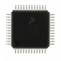
MC9S08DV32ACLF Freescale Semiconductor, MC9S08DV32ACLF Datasheet - Page 331

MC9S08DV32ACLF
Manufacturer Part Number
MC9S08DV32ACLF
Description
IC MCU 32K FLASH 2K RAM 48-LQFP
Manufacturer
Freescale Semiconductor
Series
HCS08r
Specifications of MC9S08DV32ACLF
Core Processor
HCS08
Core Size
8-Bit
Speed
40MHz
Connectivity
CAN, I²C, LIN, SCI, SPI
Peripherals
LVD, POR, PWM, WDT
Number Of I /o
39
Program Memory Size
32KB (32K x 8)
Program Memory Type
FLASH
Ram Size
2K x 8
Voltage - Supply (vcc/vdd)
2.7 V ~ 5.5 V
Data Converters
A/D 16x12b
Oscillator Type
External
Operating Temperature
-40°C ~ 85°C
Package / Case
48-LQFP
Processor Series
S08DV
Core
HCS08
Data Bus Width
8 bit
Data Ram Size
2 KB
Interface Type
CAN, I2C, SCI, SPI
Number Of Programmable I/os
26
Operating Supply Voltage
5.5 V
Mounting Style
SMD/SMT
3rd Party Development Tools
EWS08
Development Tools By Supplier
DEMO9S08DZ60
On-chip Adc
12 bit, 10 channel
Controller Family/series
HCS08
No. Of I/o's
39
Ram Memory Size
2KB
Cpu Speed
40MHz
No. Of Timers
2
Digital Ic Case Style
LQFP
Rohs Compliant
Yes
Lead Free Status / RoHS Status
Lead free / RoHS Compliant
Eeprom Size
-
Lead Free Status / Rohs Status
Lead free / RoHS Compliant
Available stocks
Company
Part Number
Manufacturer
Quantity
Price
Company:
Part Number:
MC9S08DV32ACLF
Manufacturer:
Freescale Semiconductor
Quantity:
10 000
- Current page: 331 of 414
- Download datasheet (5Mb)
In input capture mode, reading either byte (TPMxCnVH or TPMxCnVL) latches the contents of both bytes
into a buffer where they remain latched until the other half is read. This latching mechanism also resets
(becomes unlatched) when the TPMxCnSC register is written (whether BDM mode is active or not). Any
write to the channel registers will be ignored during the input capture mode.
When BDM is active, the coherency mechanism is frozen (unless reset by writing to TPMxCnSC register)
such that the buffer latches remain in the state they were in when the BDM became active, even if one or
both halves of the channel register are read while BDM is active. This assures that if the user was in the
middle of reading a 16-bit register when BDM became active, it will read the appropriate value from the
other half of the 16-bit value after returning to normal execution. The value read from the TPMxCnVH
and TPMxCnVL registers in BDM mode is the value of these registers and not the value of their read
buffer.
In output compare or PWM modes, writing to either byte (TPMxCnVH or TPMxCnVL) latches the value
into a buffer. After both bytes are written, they are transferred as a coherent 16-bit value into the
timer-channel registers according to the value of CLKSB:CLKSA bits and the selected mode, so:
The latching mechanism may be manually reset by writing to the TPMxCnSC register (whether BDM
mode is active or not). This latching mechanism allows coherent 16-bit writes in either big-endian or
little-endian order which is friendly to various compiler implementations.
When BDM is active, the coherency mechanism is frozen such that the buffer latches remain in the state
they were in when the BDM became active even if one or both halves of the channel register are written
while BDM is active. Any write to the channel registers bypasses the buffer latches and directly write to
the channel register while BDM is active. The values written to the channel register while BDM is active
Freescale Semiconductor
Reset
Reset
•
•
•
W
W
R
R
If (CLKSB:CLKSA = 0:0), then the registers are updated when the second byte is written.
If (CLKSB:CLKSA not = 0:0 and in output compare mode) then the registers are updated after the
second byte is written and on the next change of the TPM counter (end of the prescaler counting).
If (CLKSB:CLKSA not = 0:0 and in EPWM or CPWM modes), then the registers are updated after
the both bytes were written, and the TPM counter changes from (TPMxMODH:TPMxMODL - 1)
to (TPMxMODH:TPMxMODL). If the TPM counter is a free-running counter then the update is
made when the TPM counter changes from 0xFFFE to 0xFFFF.
Bit 15
Bit 7
0
0
7
7
Figure 16-13. TPM Channel Value Register High (TPMxCnVH)
Figure 16-14. TPM Channel Value Register Low (TPMxCnVL)
14
0
6
0
6
6
MC9S08DV60 Series Data Sheet, Rev 3
13
5
0
5
5
0
12
0
4
0
4
4
11
0
3
0
3
3
Chapter 16 Timer/PWM Module (S08TPMV3)
10
0
2
0
2
2
1
9
0
1
1
0
Bit 8
Bit 0
0
0
0
0
331
Related parts for MC9S08DV32ACLF
Image
Part Number
Description
Manufacturer
Datasheet
Request
R
Part Number:
Description:
Manufacturer:
Freescale Semiconductor, Inc
Datasheet:
Part Number:
Description:
Manufacturer:
Freescale Semiconductor, Inc
Datasheet:
Part Number:
Description:
Manufacturer:
Freescale Semiconductor, Inc
Datasheet:
Part Number:
Description:
Manufacturer:
Freescale Semiconductor, Inc
Datasheet:
Part Number:
Description:
Manufacturer:
Freescale Semiconductor, Inc
Datasheet:
Part Number:
Description:
Manufacturer:
Freescale Semiconductor, Inc
Datasheet:
Part Number:
Description:
Manufacturer:
Freescale Semiconductor, Inc
Datasheet:
Part Number:
Description:
Manufacturer:
Freescale Semiconductor, Inc
Datasheet:
Part Number:
Description:
Manufacturer:
Freescale Semiconductor, Inc
Datasheet:
Part Number:
Description:
Manufacturer:
Freescale Semiconductor, Inc
Datasheet:
Part Number:
Description:
Manufacturer:
Freescale Semiconductor, Inc
Datasheet:
Part Number:
Description:
Manufacturer:
Freescale Semiconductor, Inc
Datasheet:
Part Number:
Description:
Manufacturer:
Freescale Semiconductor, Inc
Datasheet:
Part Number:
Description:
Manufacturer:
Freescale Semiconductor, Inc
Datasheet:
Part Number:
Description:
Manufacturer:
Freescale Semiconductor, Inc
Datasheet:


