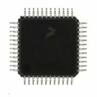
MC9S08DV32ACLF Freescale Semiconductor, MC9S08DV32ACLF Datasheet - Page 346

MC9S08DV32ACLF
Manufacturer Part Number
MC9S08DV32ACLF
Description
IC MCU 32K FLASH 2K RAM 48-LQFP
Manufacturer
Freescale Semiconductor
Series
HCS08r
Specifications of MC9S08DV32ACLF
Core Processor
HCS08
Core Size
8-Bit
Speed
40MHz
Connectivity
CAN, I²C, LIN, SCI, SPI
Peripherals
LVD, POR, PWM, WDT
Number Of I /o
39
Program Memory Size
32KB (32K x 8)
Program Memory Type
FLASH
Ram Size
2K x 8
Voltage - Supply (vcc/vdd)
2.7 V ~ 5.5 V
Data Converters
A/D 16x12b
Oscillator Type
External
Operating Temperature
-40°C ~ 85°C
Package / Case
48-LQFP
Processor Series
S08DV
Core
HCS08
Data Bus Width
8 bit
Data Ram Size
2 KB
Interface Type
CAN, I2C, SCI, SPI
Number Of Programmable I/os
26
Operating Supply Voltage
5.5 V
Mounting Style
SMD/SMT
3rd Party Development Tools
EWS08
Development Tools By Supplier
DEMO9S08DZ60
On-chip Adc
12 bit, 10 channel
Controller Family/series
HCS08
No. Of I/o's
39
Ram Memory Size
2KB
Cpu Speed
40MHz
No. Of Timers
2
Digital Ic Case Style
LQFP
Rohs Compliant
Yes
Lead Free Status / RoHS Status
Lead free / RoHS Compliant
Eeprom Size
-
Lead Free Status / Rohs Status
Lead free / RoHS Compliant
Available stocks
Company
Part Number
Manufacturer
Quantity
Price
Company:
Part Number:
MC9S08DV32ACLF
Manufacturer:
Freescale Semiconductor
Quantity:
10 000
- Current page: 346 of 414
- Download datasheet (5Mb)
Chapter 17 Development Support
17.1.2
Features of the BDC module include:
Features of the ICE system include:
17.2
All MCUs in the HCS08 Family contain a single-wire background debug interface that supports in-circuit
programming of on-chip nonvolatile memory and sophisticated non-intrusive debug capabilities. Unlike
debug interfaces on earlier 8-bit MCUs, this system does not interfere with normal application resources.
It does not use any user memory or locations in the memory map and does not share any on-chip
peripherals.
BDC commands are divided into two groups:
346
•
•
•
•
•
•
•
•
•
•
•
•
•
•
•
Single pin for mode selection and background communications
BDC registers are not located in the memory map
SYNC command to determine target communications rate
Non-intrusive commands for memory access
Active background mode commands for CPU register access
GO and TRACE1 commands
BACKGROUND command can wake CPU from stop or wait modes
One hardware address breakpoint built into BDC
Oscillator runs in stop mode, if BDC enabled
COP watchdog disabled while in active background mode
Two trigger comparators: Two address + read/write (R/W) or one full address + data + R/W
Flexible 8-word by 16-bit FIFO (first-in, first-out) buffer for capture information:
— Change-of-flow addresses or
— Event-only data
Two types of breakpoints:
— Tag breakpoints for instruction opcodes
— Force breakpoints for any address access
Nine trigger modes:
— Basic: A-only, A OR B
— Sequence: A then B
— Full: A AND B data, A AND NOT B data
— Event (store data): Event-only B, A then event-only B
— Range: Inside range (A ≤ address ≤ B), outside range (address < A or address > B)
Active background mode commands require that the target MCU is in active background mode (the
user program is not running). Active background mode commands allow the CPU registers to be
read or written, and allow the user to trace one user instruction at a time, or GO to the user program
from active background mode.
Background Debug Controller (BDC)
Features
MC9S08DV60 Series Data Sheet, Rev 3
Freescale Semiconductor
Related parts for MC9S08DV32ACLF
Image
Part Number
Description
Manufacturer
Datasheet
Request
R
Part Number:
Description:
Manufacturer:
Freescale Semiconductor, Inc
Datasheet:
Part Number:
Description:
Manufacturer:
Freescale Semiconductor, Inc
Datasheet:
Part Number:
Description:
Manufacturer:
Freescale Semiconductor, Inc
Datasheet:
Part Number:
Description:
Manufacturer:
Freescale Semiconductor, Inc
Datasheet:
Part Number:
Description:
Manufacturer:
Freescale Semiconductor, Inc
Datasheet:
Part Number:
Description:
Manufacturer:
Freescale Semiconductor, Inc
Datasheet:
Part Number:
Description:
Manufacturer:
Freescale Semiconductor, Inc
Datasheet:
Part Number:
Description:
Manufacturer:
Freescale Semiconductor, Inc
Datasheet:
Part Number:
Description:
Manufacturer:
Freescale Semiconductor, Inc
Datasheet:
Part Number:
Description:
Manufacturer:
Freescale Semiconductor, Inc
Datasheet:
Part Number:
Description:
Manufacturer:
Freescale Semiconductor, Inc
Datasheet:
Part Number:
Description:
Manufacturer:
Freescale Semiconductor, Inc
Datasheet:
Part Number:
Description:
Manufacturer:
Freescale Semiconductor, Inc
Datasheet:
Part Number:
Description:
Manufacturer:
Freescale Semiconductor, Inc
Datasheet:
Part Number:
Description:
Manufacturer:
Freescale Semiconductor, Inc
Datasheet:


