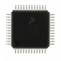
MC9S08DV32ACLF Freescale Semiconductor, MC9S08DV32ACLF Datasheet - Page 345

MC9S08DV32ACLF
Manufacturer Part Number
MC9S08DV32ACLF
Description
IC MCU 32K FLASH 2K RAM 48-LQFP
Manufacturer
Freescale Semiconductor
Series
HCS08r
Specifications of MC9S08DV32ACLF
Core Processor
HCS08
Core Size
8-Bit
Speed
40MHz
Connectivity
CAN, I²C, LIN, SCI, SPI
Peripherals
LVD, POR, PWM, WDT
Number Of I /o
39
Program Memory Size
32KB (32K x 8)
Program Memory Type
FLASH
Ram Size
2K x 8
Voltage - Supply (vcc/vdd)
2.7 V ~ 5.5 V
Data Converters
A/D 16x12b
Oscillator Type
External
Operating Temperature
-40°C ~ 85°C
Package / Case
48-LQFP
Processor Series
S08DV
Core
HCS08
Data Bus Width
8 bit
Data Ram Size
2 KB
Interface Type
CAN, I2C, SCI, SPI
Number Of Programmable I/os
26
Operating Supply Voltage
5.5 V
Mounting Style
SMD/SMT
3rd Party Development Tools
EWS08
Development Tools By Supplier
DEMO9S08DZ60
On-chip Adc
12 bit, 10 channel
Controller Family/series
HCS08
No. Of I/o's
39
Ram Memory Size
2KB
Cpu Speed
40MHz
No. Of Timers
2
Digital Ic Case Style
LQFP
Rohs Compliant
Yes
Lead Free Status / RoHS Status
Lead free / RoHS Compliant
Eeprom Size
-
Lead Free Status / Rohs Status
Lead free / RoHS Compliant
Available stocks
Company
Part Number
Manufacturer
Quantity
Price
Company:
Part Number:
MC9S08DV32ACLF
Manufacturer:
Freescale Semiconductor
Quantity:
10 000
- Current page: 345 of 414
- Download datasheet (5Mb)
Chapter 17
Development Support
17.1
Introduction
Development support systems in the HCS08 include the background debug controller (BDC) and the
on-chip debug module (DBG). The BDC provides a single-wire debug interface to the target MCU that
provides a convenient interface for programming the on-chip Flash and other nonvolatile memories. The
BDC is also the primary debug interface for development and allows non-intrusive access to memory data
and traditional debug features such as CPU register modify, breakpoints, and single instruction trace
commands.
In the HCS08 Family, address and data bus signals are not available on external pins (not even in test
modes). Debug is done through commands fed into the target MCU via the single-wire background debug
interface. The debug module provides a means to selectively trigger and capture bus information so an
external development system can reconstruct what happened inside the MCU on a cycle-by-cycle basis
without having external access to the address and data signals.
17.1.1
Forcing Active Background
The method for forcing active background mode depends on the specific HCS08 derivative. For the
MC9S08DV60, you can force active background after a power-on reset by holding the BKGD pin low as
the device exits the reset condition. You can also force active background by driving BKGD low
immediately after a serial background command that writes a one to the BDFR bit in the SBDFR register.
If no debug pod is connected to the BKGD pin, the MCU will always reset into normal operating mode.
MC9S08DV60 Series Data Sheet, Rev 3
Freescale Semiconductor
345
Related parts for MC9S08DV32ACLF
Image
Part Number
Description
Manufacturer
Datasheet
Request
R
Part Number:
Description:
Manufacturer:
Freescale Semiconductor, Inc
Datasheet:
Part Number:
Description:
Manufacturer:
Freescale Semiconductor, Inc
Datasheet:
Part Number:
Description:
Manufacturer:
Freescale Semiconductor, Inc
Datasheet:
Part Number:
Description:
Manufacturer:
Freescale Semiconductor, Inc
Datasheet:
Part Number:
Description:
Manufacturer:
Freescale Semiconductor, Inc
Datasheet:
Part Number:
Description:
Manufacturer:
Freescale Semiconductor, Inc
Datasheet:
Part Number:
Description:
Manufacturer:
Freescale Semiconductor, Inc
Datasheet:
Part Number:
Description:
Manufacturer:
Freescale Semiconductor, Inc
Datasheet:
Part Number:
Description:
Manufacturer:
Freescale Semiconductor, Inc
Datasheet:
Part Number:
Description:
Manufacturer:
Freescale Semiconductor, Inc
Datasheet:
Part Number:
Description:
Manufacturer:
Freescale Semiconductor, Inc
Datasheet:
Part Number:
Description:
Manufacturer:
Freescale Semiconductor, Inc
Datasheet:
Part Number:
Description:
Manufacturer:
Freescale Semiconductor, Inc
Datasheet:
Part Number:
Description:
Manufacturer:
Freescale Semiconductor, Inc
Datasheet:
Part Number:
Description:
Manufacturer:
Freescale Semiconductor, Inc
Datasheet:


