D6417709SHF200BV Renesas Electronics America, D6417709SHF200BV Datasheet - Page 21
D6417709SHF200BV
Manufacturer Part Number
D6417709SHF200BV
Description
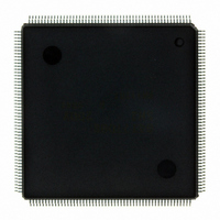
IC SUPER H MPU ROMLESS 208LQFP
Manufacturer
Renesas Electronics America
Series
SuperH® SH7700r
Datasheet
1.D6417709SBP167BV.pdf
(809 pages)
Specifications of D6417709SHF200BV
Core Processor
SH-3
Core Size
32-Bit
Speed
200MHz
Connectivity
EBI/EMI, FIFO, IrDA, SCI, SmartCard
Peripherals
DMA, POR, WDT
Number Of I /o
96
Program Memory Type
ROMless
Ram Size
16K x 8
Voltage - Supply (vcc/vdd)
1.85 V ~ 2.15 V
Data Converters
A/D 8x10b; D/A 2x8b
Oscillator Type
Internal
Operating Temperature
-20°C ~ 75°C
Package / Case
208-QFP Exposed Pad, 208-eQFP, 208-HQFP
Lead Free Status / RoHS Status
Lead free / RoHS Compliant
Eeprom Size
-
Program Memory Size
-
Available stocks
Company
Part Number
Manufacturer
Quantity
Price
Company:

Part Number:
D6417709SHF200BV
Manufacturer:
Renesas Electronics America
Quantity:
10 000


5.2
5.3
5.4
Section 6 Interrupt Controller (INTC)
6.1
6.2
6.3
6.4
6.5
5.1.2
5.1.3
Register Description .......................................................................................................... 105
5.2.1
5.2.2
Cache Operation ................................................................................................................ 109
5.3.1
5.3.2
5.3.3
5.3.4
5.3.5
5.3.6
Memory-Mapped Cache.................................................................................................... 112
5.4.1
5.4.2
5.4.3
Overview ........................................................................................................................... 117
6.1.1
6.1.2
6.1.3
6.1.4
Interrupt Sources ............................................................................................................... 121
6.2.1
6.2.2
6.2.3
6.2.4
6.2.5
6.2.6
INTC Registers.................................................................................................................. 131
6.3.1
6.3.2
6.3.3
6.3.4
6.3.5
6.3.6
6.3.7
6.3.8
INTC Operation................................................................................................................. 143
6.4.1
6.4.2
Interrupt Response Time ................................................................................................... 145
Write Access ........................................................................................................ 111
Features ................................................................................................................ 117
Pin Configuration ................................................................................................. 119
Interrupt Exception Handling and Priority ........................................................... 125
Multiple Interrupts................................................................................................ 145
Cache Structure .................................................................................................... 103
Register Configuration ......................................................................................... 105
Cache Control Register (CCR) ............................................................................. 105
Cache Control Register 2 (CCR2) ........................................................................ 106
Searching the Cache ............................................................................................. 109
Read Access ......................................................................................................... 111
Prefetch Operation................................................................................................ 111
Write-Back Buffer................................................................................................ 111
Coherency of Cache and External Memory.......................................................... 112
Address Array ...................................................................................................... 112
Data Array ............................................................................................................ 113
Examples of Usage ............................................................................................... 115
Block Diagram ..................................................................................................... 118
Register Configuration ......................................................................................... 120
NMI Interrupt ....................................................................................................... 121
IRQ Interrupts ...................................................................................................... 121
IRL Interrupts....................................................................................................... 122
PINT Interrupts .................................................................................................... 124
On-Chip Peripheral Module Interrupts................................................................. 124
Interrupt Priority Registers A to E (IPRA–IPRE) ................................................ 131
Interrupt Control Register 0 (ICR0) ..................................................................... 132
Interrupt Control Register 1 (ICR1) ..................................................................... 133
Interrupt Control Register 2 (ICR2) ..................................................................... 136
PINT Interrupt Enable Register (PINTER) .......................................................... 137
Interrupt Request Register 0 (IRR0)..................................................................... 138
Interrupt Request Register 1 (IRR1)..................................................................... 140
Interrupt Request Register 2 (IRR2)..................................................................... 141
Interrupt Sequence................................................................................................ 143
........................................................................... 117
Rev. 5.00, 09/03, page xix of xliv
Related parts for D6417709SHF200BV
Image
Part Number
Description
Manufacturer
Datasheet
Request
R

Part Number:
Description:
KIT STARTER FOR M16C/29
Manufacturer:
Renesas Electronics America
Datasheet:

Part Number:
Description:
KIT STARTER FOR R8C/2D
Manufacturer:
Renesas Electronics America
Datasheet:

Part Number:
Description:
R0K33062P STARTER KIT
Manufacturer:
Renesas Electronics America
Datasheet:

Part Number:
Description:
KIT STARTER FOR R8C/23 E8A
Manufacturer:
Renesas Electronics America
Datasheet:

Part Number:
Description:
KIT STARTER FOR R8C/25
Manufacturer:
Renesas Electronics America
Datasheet:

Part Number:
Description:
KIT STARTER H8S2456 SHARPE DSPLY
Manufacturer:
Renesas Electronics America
Datasheet:

Part Number:
Description:
KIT STARTER FOR R8C38C
Manufacturer:
Renesas Electronics America
Datasheet:

Part Number:
Description:
KIT STARTER FOR R8C35C
Manufacturer:
Renesas Electronics America
Datasheet:

Part Number:
Description:
KIT STARTER FOR R8CL3AC+LCD APPS
Manufacturer:
Renesas Electronics America
Datasheet:
Part Number:
Description:
KIT STARTER FOR RX610
Manufacturer:
Renesas Electronics America
Datasheet:

Part Number:
Description:
KIT STARTER FOR R32C/118
Manufacturer:
Renesas Electronics America
Datasheet:

Part Number:
Description:
KIT DEV RSK-R8C/26-29
Manufacturer:
Renesas Electronics America
Datasheet:

Part Number:
Description:
KIT STARTER FOR SH7124
Manufacturer:
Renesas Electronics America
Datasheet:

Part Number:
Description:
KIT STARTER FOR H8SX/1622
Manufacturer:
Renesas Electronics America
Datasheet:

Part Number:
Description:
KIT DEV FOR SH7203
Manufacturer:
Renesas Electronics America
Datasheet: