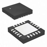
ATTINY44-15MZ Atmel, ATTINY44-15MZ Datasheet - Page 108

ATTINY44-15MZ
Manufacturer Part Number
ATTINY44-15MZ
Description
MCU AVR 4K FLASH 15MHZ 20-QFN
Manufacturer
Atmel
Series
AVR® ATtinyr
Datasheet
1.ATTINY44-15MZ.pdf
(225 pages)
Specifications of ATTINY44-15MZ
Package / Case
20-QFN Exposed Pad
Voltage - Supply (vcc/vdd)
2.7 V ~ 5.5 V
Operating Temperature
-40°C ~ 125°C
Speed
16MHz
Number Of I /o
12
Eeprom Size
256 x 8
Core Processor
AVR
Program Memory Type
FLASH
Ram Size
256 x 8
Program Memory Size
4KB (4K x 8)
Data Converters
A/D 8x10b
Oscillator Type
Internal
Peripherals
Brown-out Detect/Reset, POR, PWM, WDT
Connectivity
USI
Core Size
8-Bit
Processor Series
ATTINY4x
Core
AVR8
Data Bus Width
8 bit
Data Ram Size
256 B
Interface Type
SPI, UART
Maximum Clock Frequency
16 MHz
Number Of Programmable I/os
12
Number Of Timers
2
Maximum Operating Temperature
+ 85 C
Mounting Style
SMD/SMT
3rd Party Development Tools
EWAVR, EWAVR-BL
Development Tools By Supplier
ATAVRDRAGON, ATSTK500, ATSTK600, ATAVRISP2, ATAVRONEKIT
Minimum Operating Temperature
- 40 C
On-chip Adc
10 bit, 8 Channel
Lead Free Status / RoHS Status
Lead free / RoHS Compliant
Available stocks
Company
Part Number
Manufacturer
Quantity
Price
Company:
Part Number:
ATTINY44-15MZ
Manufacturer:
ATMEL
Quantity:
1 000
Part Number:
ATTINY44-15MZ
Manufacturer:
ATMEL/爱特梅尔
Quantity:
20 000
14.9.5
108
Atmel ATtiny24/44/84 [Preliminary]
Phase and Frequency Correct PWM Mode
The timer/counter overflow flag (TOV1) is set each time the counter reaches bottom. When
either OCR1A or ICR1 is used for defining the TOP value, the OC1A or ICF1 flag is set
accordingly on the same timer clock cycle on which the OCR1x registers are updated with the
double buffer value (at top). The interrupt flags can be used to generate an interrupt each time
the counter reaches the top or bottom value.
When changing the top value, the program must ensure that the new top value is higher or
equal to the value of all of the compare registers. If the top value is lower than any of the com-
pare registers, a compare match will never occur between TCNT1 and OCR1x. Note that
when using fixed top values, the unused bits are masked to zero when any of the OCR1x reg-
isters are written. As the third period shown in
the top actively while the timer/counter is running in the phase correct mode can result in an
asymmetrical output. The reason for this can be found in the time of update of the OCR1x reg-
ister. Since the OCR1x update occurs at top, the PWM period starts and ends at top. This
implies that the length of the falling slope is determined by the previous top value, while the
length of the rising slope is determined by the new top value. When these two values differ,
the two slopes of the period will differ in length. The difference in length gives the asymmetri-
cal result on the output.
It is recommended to use the phase and frequency correct mode instead of the phase correct
mode when changing the top value while the timer/counter is running. When using a static top
value, there are practically no differences between the two modes of operation.
In phase correct PWM mode, the compare units allow generation of PWM waveforms on the
OC1x pins. Setting the COM1x1:0 bits to two will produce a non-inverted PWM, and an
inverted PWM output can be generated by setting the COM1x1:0 to three (See
page
the port pin is set as output (DDR_OC1x). The PWM waveform is generated by setting (or
clearing) the OC1x register at the compare match between OCR1x and TCNT1 when the
counter increments, and clearing (or setting) the OC1x register at compare match between
OCR1x and TCNT1 when the counter decrements. The PWM frequency for the output when
using phase correct PWM can be calculated by the following equation:
The variable N represents the prescaler divider (1, 8, 64, 256, or 1024).
The extreme values for the OCR1x register represent special cases when generating a PWM
waveform output in the phase correct PWM mode. If the OCR1x is set equal to bottom, the
output will be continuously low, and if set equal to top, the output will be continuously high for
non-inverted PWM mode. For inverted PWM the output will have the opposite logic values.
The phase and frequency correct pulse width modulation, or phase and frequency correct
PWM, mode (WGM13:0 = 8 or 9) provides a high-resolution phase and frequency correct
PWM waveform generation option. The phase and frequency correct PWM mode is, like the
phase correct PWM mode, based on a dual-slope operation. The counter counts repeatedly
from bottom (0x0000) to top and then from top to bottom. In non-inverting compare output
mode, the output compare (OC1x) is cleared on the compare match between TCNT1 and
OCR1x while up-counting, and set on the compare match while down-counting.
114). The actual OC1x value will only be visible on the port pin if the data direction for
f
OCnxPCPWM
=
Figure 14-8 on page 107
---------------------------------
2
f
clk_I/O
N
TOP
illustrates, changing
Table 14-3 on
7701E–AVR–02/11


