ATTINY44-15MZ Atmel, ATTINY44-15MZ Datasheet - Page 149
ATTINY44-15MZ
Manufacturer Part Number
ATTINY44-15MZ
Description
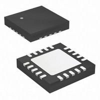
MCU AVR 4K FLASH 15MHZ 20-QFN
Manufacturer
Atmel
Series
AVR® ATtinyr
Datasheet
1.ATTINY44-15MZ.pdf
(225 pages)
Specifications of ATTINY44-15MZ
Package / Case
20-QFN Exposed Pad
Voltage - Supply (vcc/vdd)
2.7 V ~ 5.5 V
Operating Temperature
-40°C ~ 125°C
Speed
16MHz
Number Of I /o
12
Eeprom Size
256 x 8
Core Processor
AVR
Program Memory Type
FLASH
Ram Size
256 x 8
Program Memory Size
4KB (4K x 8)
Data Converters
A/D 8x10b
Oscillator Type
Internal
Peripherals
Brown-out Detect/Reset, POR, PWM, WDT
Connectivity
USI
Core Size
8-Bit
Processor Series
ATTINY4x
Core
AVR8
Data Bus Width
8 bit
Data Ram Size
256 B
Interface Type
SPI, UART
Maximum Clock Frequency
16 MHz
Number Of Programmable I/os
12
Number Of Timers
2
Maximum Operating Temperature
+ 85 C
Mounting Style
SMD/SMT
3rd Party Development Tools
EWAVR, EWAVR-BL
Development Tools By Supplier
ATAVRDRAGON, ATSTK500, ATSTK600, ATAVRISP2, ATAVRONEKIT
Minimum Operating Temperature
- 40 C
On-chip Adc
10 bit, 8 Channel
Lead Free Status / RoHS Status
Lead free / RoHS Compliant
Available stocks
Company
Part Number
Manufacturer
Quantity
Price
Company:

Part Number:
ATTINY44-15MZ
Manufacturer:
ATMEL
Quantity:
1 000
Part Number:
ATTINY44-15MZ
Manufacturer:
ATMEL/爱特梅尔
Quantity:
20 000


18.10 Register Description
18.10.1
7701E–AVR–02/11
ADMUX – ADC Multiplexer Selection Register
To obtain best accuracy the coefficient k should be measured using two temperature calibra-
tions. Using offset calibration, set k = 1.0, where k = (1024*1.07mV/°C)/1.1V~1.0 [1/°C].
• Bit 7:6 – REFS1:REFS0: Reference Selection Bits
These bits select the voltage reference for the ADC, as shown in
these bits are changed during a conversion, the change will not go in effect until this
conversion is complete (ADIF in ADCSR is set).
Special care should be taken when changing differential channels. Once a differential channel
has been selected, the stage may take as much as 25 ADC clock cycles to stabilize to the new
value. Thus conversions should not be started within the first 13 clock cycles after selecting a
new differential channel. Alternatively, conversion results obtained within this period should be
discarded.
The same settling time should be observed for the first differential conversion after changing
ADC reference (by changing the REFS1:0 bits in the ADMUX register).
For channels where differential gain is used (i.e., the gain stage), using VCC or an optional
external AREF higher than (VCC - 1V) is not recommended, as this will affect ADC accuracy.
The internal voltage reference may not be connected to the AREF pin if an external voltage is
already being applied to it. The internal voltage reference is connected to the AREF pin when
REFS1:0 is set to the value "11".
Table 18-3.
• Bits 5:0 – MUX5:0: Analog Channel and Gain Selection Bits
The value of these bits selects which combination of analog inputs are connected to the ADC.
In the case of differential input, gain selection is also made with these bits. Selections on
18-4 on page 150
and the offset calibration selections are located. Selecting the single-ended channel ADC8
enables the temperature measurement. See
are changed during a conversion, the change will not go into effect until this conversion is
complete (ADIF in ADCSRA is set).
Bit
0x07 (0x27)
Read/Write
Initial Value
REFS1
0
0
1
1
Voltage Reference Selections for ADC
REFS1
REFS0
R/W
7
0
0
1
0
1
show values for single-ended channels and where the differential channels
REFS0
R/W
6
0
Voltage Reference Selection
V
External Voltage Reference at PA0 (AREF) pin, Internal Voltage Reference
turned off.
Internal 1.1V Voltage Reference.
Reserved.
Atmel ATtiny24/44/84 [Preliminary]
CC
used as analog reference, disconnected from PA0 (AREF).
MUX5
R/W
5
0
MUX4
R/W
4
0
Table 18-4 on page 150
MUX3
R/W
3
0
MUX2
R/W
2
0
Table 18-3 on page
MUX1
R/W
1
0
ffor details. If these bits
MUX0
R/W
0
0
ADMUX
149. If
Table
149
Related parts for ATTINY44-15MZ
Image
Part Number
Description
Manufacturer
Datasheet
Request
R

Part Number:
Description:
Manufacturer:
Atmel Corporation
Datasheet:
Part Number:
Description:
Manufacturer:
Atmel Corporation
Datasheet:

Part Number:
Description:
IC MCU AVR 4K FLASH 20MHZ 20-QFN
Manufacturer:
Atmel
Datasheet:

Part Number:
Description:
IC MCU AVR 4K FLASH 20MHZ 14SOIC
Manufacturer:
Atmel
Datasheet:

Part Number:
Description:
MCU AVR 4KB FLASH 20MHZ 14SOIC
Manufacturer:
Atmel
Datasheet:
Part Number:
Description:
MCU AVR 4KB FLASH 20MHZ 20QFN
Manufacturer:
Atmel
Datasheet:
Part Number:
Description:
IC MCU AVR 4K FLASH 15MHZ 14SOIC
Manufacturer:
Atmel
Datasheet:

Part Number:
Description:
IC MCU AVR 4K FLASH 20MHZ 14-DIP
Manufacturer:
Atmel
Datasheet:
Part Number:
Description:
Manufacturer:
Atmel Corporation
Datasheet:
Part Number:
Description:
Microcontrollers (MCU) 512B FL 32B SRAM TIMER ATTINY4 12MHz
Manufacturer:
Atmel
Part Number:
Description:
IC MCU AVR 512B FLASH SOT-23-6
Manufacturer:
Atmel
Datasheet:

Part Number:
Description:
IC MCU AVR 512B FLASH SOT-23-6
Manufacturer:
Atmel
Datasheet: