ATTINY44-15MZ Atmel, ATTINY44-15MZ Datasheet - Page 72
ATTINY44-15MZ
Manufacturer Part Number
ATTINY44-15MZ
Description
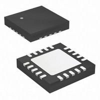
MCU AVR 4K FLASH 15MHZ 20-QFN
Manufacturer
Atmel
Series
AVR® ATtinyr
Datasheet
1.ATTINY44-15MZ.pdf
(225 pages)
Specifications of ATTINY44-15MZ
Package / Case
20-QFN Exposed Pad
Voltage - Supply (vcc/vdd)
2.7 V ~ 5.5 V
Operating Temperature
-40°C ~ 125°C
Speed
16MHz
Number Of I /o
12
Eeprom Size
256 x 8
Core Processor
AVR
Program Memory Type
FLASH
Ram Size
256 x 8
Program Memory Size
4KB (4K x 8)
Data Converters
A/D 8x10b
Oscillator Type
Internal
Peripherals
Brown-out Detect/Reset, POR, PWM, WDT
Connectivity
USI
Core Size
8-Bit
Processor Series
ATTINY4x
Core
AVR8
Data Bus Width
8 bit
Data Ram Size
256 B
Interface Type
SPI, UART
Maximum Clock Frequency
16 MHz
Number Of Programmable I/os
12
Number Of Timers
2
Maximum Operating Temperature
+ 85 C
Mounting Style
SMD/SMT
3rd Party Development Tools
EWAVR, EWAVR-BL
Development Tools By Supplier
ATAVRDRAGON, ATSTK500, ATSTK600, ATAVRISP2, ATAVRONEKIT
Minimum Operating Temperature
- 40 C
On-chip Adc
10 bit, 8 Channel
Lead Free Status / RoHS Status
Lead free / RoHS Compliant
Available stocks
Company
Part Number
Manufacturer
Quantity
Price
Company:

Part Number:
ATTINY44-15MZ
Manufacturer:
ATMEL
Quantity:
1 000
Part Number:
ATTINY44-15MZ
Manufacturer:
ATMEL/爱特梅尔
Quantity:
20 000


13. 8-bit Timer/Counter0 with PWM
13.1
13.2
13.2.1
72
Features
Overview
Atmel ATtiny24/44/84 [Preliminary]
Registers
•
•
•
•
•
•
•
Timer/counter 0 is a general purpose 8-bit timer/counter module, with two independent out-
put compare units, and with PWM support. It allows accurate program execution timing (event
management) and wave generation.
A simplified block diagram of the 8-bit Timer/Counter is shown in
the actual placement of I/O pins, refer to
including I/O bits and I/O pins, are shown in bold. The device-specific I/O Register and bit
locations are listed in the
Figure 13-1. 8-bit Timer/Counter Block Diagram
The timer/counter (TCNT0) and output compare registers (OCR0A and OCR0B) are 8-bit reg-
isters. Interrupt request (abbreviated to Int.Req. in the figure) signals are all visible in the
timer/counter 0 interrupt flag register (TIFR0). All interrupts are individually masked with the
timer interrupt mask register (TIMSK0). TIFR0 and TIMSK0 are not shown in the figure.
The Timer/Counter can be clocked internally, via the prescaler, or by an external clock source
on the T0 pin. The Clock Select logic block controls which clock source and edge the
Two Independent Output Compare Units
Double Buffered Output Compare Registers
Clear Timer on Compare Match (Auto Reload)
Glitch Free, Phase Correct Pulse Width Modulator (PWM)
Variable PWM Period
Frequency Generator
Three Independent Interrupt Sources (TOV0, OCF0A, and OCF0B)
Timer/Counter
“Register Description” on page
TCCRnA
OCRnA
TCNTn
OCRnB
=
=
Direction
Count
Clear
Control Logic
Figure 1-1 on page
TOP
=
TCCRnB
Value
BOTTOM
Fixed
TOP
clk
=
Tn
0
84.
OCnA
(Int.Req.)
OCnB
(Int.Req.)
TOVn
(Int.Req.)
Clock Select
Generation
Generation
2. CPU accessible I/O Registers,
( From Prescaler )
Waveform
Waveform
Detector
Edge
Figure 13-1 on page
OCnA
OCnB
Tn
7701E–AVR–02/11
72. For
Related parts for ATTINY44-15MZ
Image
Part Number
Description
Manufacturer
Datasheet
Request
R

Part Number:
Description:
Manufacturer:
Atmel Corporation
Datasheet:
Part Number:
Description:
Manufacturer:
Atmel Corporation
Datasheet:

Part Number:
Description:
IC MCU AVR 4K FLASH 20MHZ 20-QFN
Manufacturer:
Atmel
Datasheet:

Part Number:
Description:
IC MCU AVR 4K FLASH 20MHZ 14SOIC
Manufacturer:
Atmel
Datasheet:

Part Number:
Description:
MCU AVR 4KB FLASH 20MHZ 14SOIC
Manufacturer:
Atmel
Datasheet:
Part Number:
Description:
MCU AVR 4KB FLASH 20MHZ 20QFN
Manufacturer:
Atmel
Datasheet:
Part Number:
Description:
IC MCU AVR 4K FLASH 15MHZ 14SOIC
Manufacturer:
Atmel
Datasheet:

Part Number:
Description:
IC MCU AVR 4K FLASH 20MHZ 14-DIP
Manufacturer:
Atmel
Datasheet:
Part Number:
Description:
Manufacturer:
Atmel Corporation
Datasheet:
Part Number:
Description:
Microcontrollers (MCU) 512B FL 32B SRAM TIMER ATTINY4 12MHz
Manufacturer:
Atmel
Part Number:
Description:
IC MCU AVR 512B FLASH SOT-23-6
Manufacturer:
Atmel
Datasheet:

Part Number:
Description:
IC MCU AVR 512B FLASH SOT-23-6
Manufacturer:
Atmel
Datasheet: