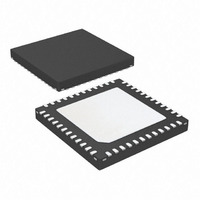
ATSAM3S4AA-MU Atmel, ATSAM3S4AA-MU Datasheet - Page 781

ATSAM3S4AA-MU
Manufacturer Part Number
ATSAM3S4AA-MU
Description
IC MCU 32BIT 256KB FLASH 48QFN
Manufacturer
Atmel
Series
SAM3Sr
Specifications of ATSAM3S4AA-MU
Core Processor
ARM® Cortex-M3™
Core Size
32-Bit
Speed
64MHz
Connectivity
I²C, MMC, SPI, SSC, UART/USART, USB
Peripherals
Brown-out Detect/Reset, DMA, I²S, POR, PWM, WDT
Number Of I /o
34
Program Memory Size
256KB (256K x 8)
Program Memory Type
FLASH
Ram Size
48K x 8
Voltage - Supply (vcc/vdd)
1.62 V ~ 1.95 V
Data Converters
A/D 8x10/12b
Oscillator Type
Internal
Operating Temperature
-40°C ~ 85°C
Package / Case
48-VQFN Exposed Pad, 48-HVQFN, 48-SQFN, 48-DHVQFN
Processor Series
ATSAM3x
Core
ARM Cortex M3
3rd Party Development Tools
JTRACE-CM3, MDK-ARM, RL-ARM, ULINK2
Development Tools By Supplier
ATSAM3S-EK
Lead Free Status / RoHS Status
Lead free / RoHS Compliant
Eeprom Size
-
Lead Free Status / Rohs Status
Details
Available stocks
Company
Part Number
Manufacturer
Quantity
Price
Part Number:
ATSAM3S4AA-MU
Manufacturer:
MICROCHIP/微芯
Quantity:
20 000
- Current page: 781 of 1118
- Download datasheet (24Mb)
34.7.11
Name:
Addresses:
Access:
This register can only be written if the WPEN bit is cleared in
• TCCLKS: Clock Selection
• CLKI: Clock Invert
0 = counter is incremented on rising edge of the clock.
1 = counter is incremented on falling edge of the clock.
• BURST: Burst Signal Selection
• CPCSTOP: Counter Clock Stopped with RC Compare
0 = counter clock is not stopped when counter reaches RC.
1 = counter clock is stopped when counter reaches RC.
6500C–ATARM–8-Feb-11
CPCDIS
Value
Value
WAVE
0
1
2
3
4
5
6
7
0
1
2
3
31
23
15
7
TC Channel Mode Register: Waveform Mode
BSWTRG
ASWTRG
Name
TIMER_CLOCK1
TIMER_CLOCK2
TIMER_CLOCK3
TIMER_CLOCK4
TIMER_CLOCK5
XC0
XC1
XC2
Name
NONE
XC0
XC1
XC2
CPCSTOP
30
22
14
TC_CMRx [x=0..2] (WAVE = 1)
0x40010004 (0)[0], 0x40010044 (0)[1], 0x40010084 (0)[2], 0x40014004 (1)[0], 0x40014044 (1)[1],
0x40014084 (1)[2]
Read-write
6
WAVSEL
Description
Clock selected: TCLK1
Clock selected: TCLK2
Clock selected: TCLK3
Clock selected: TCLK4
Clock selected: TCLK5
Clock selected: XC0
Clock selected: XC1
Clock selected: XC2
Description
The clock is not gated by an external signal.
XC0 is ANDed with the selected clock.
XC1 is ANDed with the selected clock.
XC2 is ANDed with the selected clock.
29
21
13
5
BURST
BEEVT
AEEVT
ENETRG
28
20
12
4
“TC Write Protect Mode Register” on page 778
CLKI
27
19
11
3
BCPC
ACPC
EEVT
26
18
10
2
SAM3S Preliminary
TCCLKS
25
17
9
1
EEVTEDG
BCPB
ACPA
24
16
8
0
781
Related parts for ATSAM3S4AA-MU
Image
Part Number
Description
Manufacturer
Datasheet
Request
R

Part Number:
Description:
KIT EVAL FOR ATSAM3S4C
Manufacturer:
Atmel
Datasheet:

Part Number:
Description:
Development Boards & Kits - ARM EVAL KIT SAM3S8 & SAM3SD8 series
Manufacturer:
Atmel
Datasheet:

Part Number:
Description:
AT91 ARM Cortex M3-based Processor
Manufacturer:
ATMEL [ATMEL Corporation]
Datasheet:

Part Number:
Description:
DEV KIT FOR AVR/AVR32
Manufacturer:
Atmel
Datasheet:

Part Number:
Description:
INTERVAL AND WIPE/WASH WIPER CONTROL IC WITH DELAY
Manufacturer:
ATMEL Corporation
Datasheet:

Part Number:
Description:
Low-Voltage Voice-Switched IC for Hands-Free Operation
Manufacturer:
ATMEL Corporation
Datasheet:

Part Number:
Description:
MONOLITHIC INTEGRATED FEATUREPHONE CIRCUIT
Manufacturer:
ATMEL Corporation
Datasheet:

Part Number:
Description:
AM-FM Receiver IC U4255BM-M
Manufacturer:
ATMEL Corporation
Datasheet:

Part Number:
Description:
Monolithic Integrated Feature Phone Circuit
Manufacturer:
ATMEL Corporation
Datasheet:

Part Number:
Description:
Multistandard Video-IF and Quasi Parallel Sound Processing
Manufacturer:
ATMEL Corporation
Datasheet:

Part Number:
Description:
High-performance EE PLD
Manufacturer:
ATMEL Corporation
Datasheet:

Part Number:
Description:
8-bit Flash Microcontroller
Manufacturer:
ATMEL Corporation
Datasheet:


