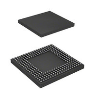
HD6417727BP100BV Renesas Electronics America, HD6417727BP100BV Datasheet - Page 157

HD6417727BP100BV
Manufacturer Part Number
HD6417727BP100BV
Description
IC SUPERH MPU ROMLESS 240BGA
Manufacturer
Renesas Electronics America
Series
SuperH® SH7700r
Datasheet
1.HD6417727BP100CV.pdf
(1098 pages)
Specifications of HD6417727BP100BV
Core Processor
SH-3 DSP
Core Size
32-Bit
Speed
100MHz
Connectivity
FIFO, SCI, SIO, SmartCard, USB
Peripherals
DMA, LCD, POR, WDT
Number Of I /o
104
Program Memory Type
ROMless
Ram Size
32K x 8
Voltage - Supply (vcc/vdd)
1.6 V ~ 2.05 V
Data Converters
A/D 6x10b; D/A 2x8b
Oscillator Type
Internal
Operating Temperature
-20°C ~ 75°C
Package / Case
240-BGA
Lead Free Status / RoHS Status
Contains lead / RoHS non-compliant
Eeprom Size
-
Program Memory Size
-
- Current page: 157 of 1098
- Download datasheet (7Mb)
3.1.3
Logical Address Space: The SH7727 uses 32-bit logical addresses to access a 4-Gbyte logical
address space that is divided into several areas. Address space mapping is shown in figure 3.2.
In the privileged mode, there are five areas, P0 to P4.
The P0 and P3 areas are mapped onto physical address space in page units, in accordance with
address translation table information. Write-back or write-through can be selected for write access
by means of a CCR setting.
Mapping of the P1 area is fixed in physical address space (H'00000000 to H'1FFFFFFF). In the
P1 area, setting a logical address MSB (bit 31) to 0 generates the corresponding physical address.
P1 area accesses can be cached, and the cache control register (CCR) is set to indicate whether to
cache or not. Write-back or write-through mode can be selected.
Process 1
SH7727 MMU
Physical
memory
Process 1
Process 1
Process 2
Process 3
Figure 3.1 MMU Functions
Physical
memory
Physical
memory
(3)
(1)
Section 3 Memory Management Unit (MMU)
Rev.6.00 Mar. 27, 2009 Page 99 of 1036
Process 1
Process 1
Process 2
Process 3
Virtual
memory
Virtual
memory
MMU
MMU
REJ09B0254-0600
Physical
memory
Physical
memory
(4)
(2)
Related parts for HD6417727BP100BV
Image
Part Number
Description
Manufacturer
Datasheet
Request
R

Part Number:
Description:
KIT STARTER FOR M16C/29
Manufacturer:
Renesas Electronics America
Datasheet:

Part Number:
Description:
KIT STARTER FOR R8C/2D
Manufacturer:
Renesas Electronics America
Datasheet:

Part Number:
Description:
R0K33062P STARTER KIT
Manufacturer:
Renesas Electronics America
Datasheet:

Part Number:
Description:
KIT STARTER FOR R8C/23 E8A
Manufacturer:
Renesas Electronics America
Datasheet:

Part Number:
Description:
KIT STARTER FOR R8C/25
Manufacturer:
Renesas Electronics America
Datasheet:

Part Number:
Description:
KIT STARTER H8S2456 SHARPE DSPLY
Manufacturer:
Renesas Electronics America
Datasheet:

Part Number:
Description:
KIT STARTER FOR R8C38C
Manufacturer:
Renesas Electronics America
Datasheet:

Part Number:
Description:
KIT STARTER FOR R8C35C
Manufacturer:
Renesas Electronics America
Datasheet:

Part Number:
Description:
KIT STARTER FOR R8CL3AC+LCD APPS
Manufacturer:
Renesas Electronics America
Datasheet:

Part Number:
Description:
KIT STARTER FOR RX610
Manufacturer:
Renesas Electronics America
Datasheet:

Part Number:
Description:
KIT STARTER FOR R32C/118
Manufacturer:
Renesas Electronics America
Datasheet:

Part Number:
Description:
KIT DEV RSK-R8C/26-29
Manufacturer:
Renesas Electronics America
Datasheet:

Part Number:
Description:
KIT STARTER FOR SH7124
Manufacturer:
Renesas Electronics America
Datasheet:

Part Number:
Description:
KIT STARTER FOR H8SX/1622
Manufacturer:
Renesas Electronics America
Datasheet:

Part Number:
Description:
KIT DEV FOR SH7203
Manufacturer:
Renesas Electronics America
Datasheet:


