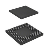
HD6417727BP100BV Renesas Electronics America, HD6417727BP100BV Datasheet - Page 44

HD6417727BP100BV
Manufacturer Part Number
HD6417727BP100BV
Description
IC SUPERH MPU ROMLESS 240BGA
Manufacturer
Renesas Electronics America
Series
SuperH® SH7700r
Datasheet
1.HD6417727BP100CV.pdf
(1098 pages)
Specifications of HD6417727BP100BV
Core Processor
SH-3 DSP
Core Size
32-Bit
Speed
100MHz
Connectivity
FIFO, SCI, SIO, SmartCard, USB
Peripherals
DMA, LCD, POR, WDT
Number Of I /o
104
Program Memory Type
ROMless
Ram Size
32K x 8
Voltage - Supply (vcc/vdd)
1.6 V ~ 2.05 V
Data Converters
A/D 6x10b; D/A 2x8b
Oscillator Type
Internal
Operating Temperature
-20°C ~ 75°C
Package / Case
240-BGA
Lead Free Status / RoHS Status
Contains lead / RoHS non-compliant
Eeprom Size
-
Program Memory Size
-
- Current page: 44 of 1098
- Download datasheet (7Mb)
Figure 17.7 Sample SCI Initialization Flowchart ...................................................................... 514
Figure 17.8 Sample Serial Transmission Flowchart .................................................................. 515
Figure 17.9 Example of Operation in Transmission in Asynchronous Mode
Figure 17.10 Sample Serial Reception Data Flowchart (1) ......................................................... 518
Figure 17.10 Sample Serial Reception Data Flowchart (2) ......................................................... 519
Figure 17.11 Example of SCI Operation in Reception
Figure 17.12 Example of Communication Using Multiprocessor Format
Figure 17.13 Sample Multiprocessor Serial Transmission Flowchart ......................................... 523
Figure 17.14 Example of SCI Operation in Transmission
Figure 17.15 Sample Multiprocessor Serial Reception Flowchart (1)......................................... 526
Figure 17.15 Sample Multiprocessor Serial Reception Flowchart (2)......................................... 527
Figure 17.16 Example of SCI Operation in Reception
Figure 17.17 Data Format in Clock Synchronous Communication............................................. 529
Figure 17.18 Sample SCI Initialization Flowchart ...................................................................... 531
Figure 17.19 Sample Serial Transmission Flowchart .................................................................. 532
Figure 17.20 Sample SCI Transmission Operation in Clocked Synchronous Mode ................... 533
Figure 17.21 Sample Serial Reception Flowchart (1).................................................................. 534
Figure 17.21 Sample Serial Reception Flowchart (2).................................................................. 535
Figure 17.22 Example of SCI Operation in Reception ................................................................ 536
Figure 17.23 Sample Flowchart of Simultaneous Serial Transmit and Receive Operations ....... 537
Figure 17.24 Receive Data Sampling Timing in Asynchronous Mode ....................................... 540
Section 18 Smart Card Interface
Figure 18.1 Smart Card Interface Block Diagram ..................................................................... 544
Figure 18.2 Pin Connection Diagram for the Smart Card Interface .......................................... 549
Figure 18.3 Data Format for Smart Card Interface.................................................................... 550
Figure 18.4 Waveform of Start Character ................................................................................. 552
Figure 18.5 Initialization Flowchart (Example)......................................................................... 556
Figure 18.6 Transmission Flowchart (Example) ....................................................................... 558
Figure 18.7 Reception Flowchart (Example)............................................................................. 560
Figure 18.8 Receive Data Sampling Timing in Smart Card Mode ............................................ 562
Figure 18.9 Retransmission in SCI Receive Mode.................................................................... 563
Figure 18.10 Retransmission in SCI Transmit Mode .................................................................. 564
Section 19 Serial Communication Interface with FIFO (SCIF)
Figure 19.1 SCIF Block Diagram.............................................................................................. 566
Rev.6.00 Mar. 27, 2009 Page xlii of lvi
REJ09B0254-0600
(Example with 8-Bit Data, Parity, One Stop Bit) ................................................... 517
(Example with 8-Bit Data, Parity, One Stop Bit) ................................................... 521
(Transmission of Data H'AA to Receiving Station A) ........................................... 522
(Example with 8-Bit Data, Multiprocessor Bit, One Stop Bit)............................... 525
(Example with 8-Bit Data, Multiprocessor Bit, One Stop Bit)............................... 528
Related parts for HD6417727BP100BV
Image
Part Number
Description
Manufacturer
Datasheet
Request
R

Part Number:
Description:
KIT STARTER FOR M16C/29
Manufacturer:
Renesas Electronics America
Datasheet:

Part Number:
Description:
KIT STARTER FOR R8C/2D
Manufacturer:
Renesas Electronics America
Datasheet:

Part Number:
Description:
R0K33062P STARTER KIT
Manufacturer:
Renesas Electronics America
Datasheet:

Part Number:
Description:
KIT STARTER FOR R8C/23 E8A
Manufacturer:
Renesas Electronics America
Datasheet:

Part Number:
Description:
KIT STARTER FOR R8C/25
Manufacturer:
Renesas Electronics America
Datasheet:

Part Number:
Description:
KIT STARTER H8S2456 SHARPE DSPLY
Manufacturer:
Renesas Electronics America
Datasheet:

Part Number:
Description:
KIT STARTER FOR R8C38C
Manufacturer:
Renesas Electronics America
Datasheet:

Part Number:
Description:
KIT STARTER FOR R8C35C
Manufacturer:
Renesas Electronics America
Datasheet:

Part Number:
Description:
KIT STARTER FOR R8CL3AC+LCD APPS
Manufacturer:
Renesas Electronics America
Datasheet:

Part Number:
Description:
KIT STARTER FOR RX610
Manufacturer:
Renesas Electronics America
Datasheet:

Part Number:
Description:
KIT STARTER FOR R32C/118
Manufacturer:
Renesas Electronics America
Datasheet:

Part Number:
Description:
KIT DEV RSK-R8C/26-29
Manufacturer:
Renesas Electronics America
Datasheet:

Part Number:
Description:
KIT STARTER FOR SH7124
Manufacturer:
Renesas Electronics America
Datasheet:

Part Number:
Description:
KIT STARTER FOR H8SX/1622
Manufacturer:
Renesas Electronics America
Datasheet:

Part Number:
Description:
KIT DEV FOR SH7203
Manufacturer:
Renesas Electronics America
Datasheet:


