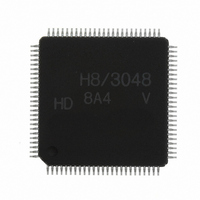
HD64F3048VTF8 Renesas Electronics America, HD64F3048VTF8 Datasheet - Page 624

HD64F3048VTF8
Manufacturer Part Number
HD64F3048VTF8
Description
IC H8 MCU FLASH 128K 100-QFP
Manufacturer
Renesas Electronics America
Series
H8® H8/300Hr
Datasheet
1.HD64F3048F16.pdf
(907 pages)
Specifications of HD64F3048VTF8
Core Processor
H8/300H
Core Size
16-Bit
Speed
8MHz
Connectivity
SCI, SmartCard
Peripherals
DMA, PWM, WDT
Number Of I /o
70
Program Memory Size
128KB (128K x 8)
Program Memory Type
FLASH
Ram Size
4K x 8
Voltage - Supply (vcc/vdd)
2.7 V ~ 5.5 V
Data Converters
A/D 8x10b; D/A 2x8b
Oscillator Type
Internal
Operating Temperature
-20°C ~ 75°C
Package / Case
100-TQFP, 100-VQFP
Lead Free Status / RoHS Status
Contains lead / RoHS non-compliant
Eeprom Size
-
Other names
HD64F3048VX8
- Current page: 624 of 907
- Download datasheet (6Mb)
Section 19 Flash Memory (H8/3048F: Dual Power Supply (V
Boot-Mode Execution Procedure: Figure 19.4 shows the boot-mode execution procedure.
Rev. 7.00 Sep 21, 2005 page 598 of 878
REJ09B0259-0700
1
2
3
4
5
6
7
8
9
10
H8/3048F transmits one H'00 byte to the
adjustment was completed successfully,
H8/3048F computes the bit rate, then
H8/3048F measures H'00 low period
sets the value in the bit rate register.
After completing bit rate adjustment,
number of program bytes (N) to be
for data transmitted from the host.
bytes to be transferred (N = N–1)
H8/3048F branches to RAM area
user program transferred to RAM
address H'FFF300 and executes
continuously at desired bit rate.
H8/3048F confirms that all flash
transmits one H'AA byte to host
H8/3048F receives, as 2 bytes,
H8/3048F calculates remaining
The host confirms that bit rate
transferred to on-chip RAM*
then transmits one H'55 byte.
boot area, then checks flash
host to indicate completion.
H8/3048F branches to RAM
Program H8/3048F pins for
memory data is H'FF, then
H8/3048F transfers part of
Host transmits H'00 data
H8/3048F transfers user
memory user area data
boot mode, and resets.
boot program to RAM
program to RAM*
Transfer end byte
All data = H'FF?
count N = 0?
Start
Yes
Yes
2
Figure 19.4 Boot Mode Flowchart
1
Delete all flash memory
blocks*
No
No
3,
*
4
1. Program the H8/3048F pins for boot mode, and start the
2. Set the host's data format to 8 bits + 1 stop bit, select the
3. H8/3048F measures the duration of repeat when the RDX
4. After H8/3048F completes SCI bit rate adjustment, one byte
5. On receiving one byte from H8/3048F to indicate completion
6. The host transmits the number of user program bytes to be
7. The H8/3048F sequentially writes the received user
8. The H8/3048F transfers part of the boot program to on-chip
9. The H8/3048F branches to the RAM boot program area
10. The H8/3048F branches to on-chip RAM address H'FFF300
Notes: 1. The user can use 3072 bytes of RAM. The number of
H8/3048F from a reset.
desired bit rate (2400, 4800 or 9600), and transmit H'00
data continuously.
pin is "Low," then computes the bit rate of the serial
transmission from the host.
of H'00 data is transmitted to indicate completion.
of bit rate adjustment, the host confirms regular reception
then transmits one byte of H'55. H8/3048F transmits H'AA to
indicate regular reception.
transferred to the H8/3048F. The number of bytes should
be sent as two bytes, upper byte followed by lower byte.
The host should then sequentially transmit the program set
by the user.
The H8/3048F transmits the received byte count and user
program sequentially to the host, one byte at a time, as
verify data (echo-back).
program to on-chip RAM area H'FFF300 to H'FFFEFF.
RAM area H'FFEF10 to H'FFF2FF.
(H'FFEF10 to H'FFF2FF) and checks for the presence of
data written in the flash memory. If data has been written in
the flash memory, the H8/3048F erases all blocks. When
erasing ends normally, the H8/3048F transmits one H'AA
byte.
and executes the user program written in that area.
2. The part of the user program that controls the flash
3. If a memory cell malfunctions and cannot be erased,
4. The allotted boot program area is H'FFF300 to
bytes transferred must not exceed 3072 bytes. Be
sure to transmit the byte length in two bytes, most
significant byte first and least significant byte second.
For example, if the byte length of the program to be
transferred is 256 bytes, (H'0100), transmit H'01 as
the most significant byte, followed by H'00 as the
least significant byte.
memory should be coded according to the flash
memory program/erase algorithms given later.
the H8/3048F transmits one H'FF byte to report an
erase error, halts erasing, and halts further
operations.
H'FFFEFF.
PP
= 12 V))
Related parts for HD64F3048VTF8
Image
Part Number
Description
Manufacturer
Datasheet
Request
R

Part Number:
Description:
KIT STARTER FOR M16C/29
Manufacturer:
Renesas Electronics America
Datasheet:

Part Number:
Description:
KIT STARTER FOR R8C/2D
Manufacturer:
Renesas Electronics America
Datasheet:

Part Number:
Description:
R0K33062P STARTER KIT
Manufacturer:
Renesas Electronics America
Datasheet:

Part Number:
Description:
KIT STARTER FOR R8C/23 E8A
Manufacturer:
Renesas Electronics America
Datasheet:

Part Number:
Description:
KIT STARTER FOR R8C/25
Manufacturer:
Renesas Electronics America
Datasheet:

Part Number:
Description:
KIT STARTER H8S2456 SHARPE DSPLY
Manufacturer:
Renesas Electronics America
Datasheet:

Part Number:
Description:
KIT STARTER FOR R8C38C
Manufacturer:
Renesas Electronics America
Datasheet:

Part Number:
Description:
KIT STARTER FOR R8C35C
Manufacturer:
Renesas Electronics America
Datasheet:

Part Number:
Description:
KIT STARTER FOR R8CL3AC+LCD APPS
Manufacturer:
Renesas Electronics America
Datasheet:

Part Number:
Description:
KIT STARTER FOR RX610
Manufacturer:
Renesas Electronics America
Datasheet:

Part Number:
Description:
KIT STARTER FOR R32C/118
Manufacturer:
Renesas Electronics America
Datasheet:

Part Number:
Description:
KIT DEV RSK-R8C/26-29
Manufacturer:
Renesas Electronics America
Datasheet:

Part Number:
Description:
KIT STARTER FOR SH7124
Manufacturer:
Renesas Electronics America
Datasheet:

Part Number:
Description:
KIT STARTER FOR H8SX/1622
Manufacturer:
Renesas Electronics America
Datasheet:


