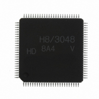
HD64F3048VTF8 Renesas Electronics America, HD64F3048VTF8 Datasheet - Page 630

HD64F3048VTF8
Manufacturer Part Number
HD64F3048VTF8
Description
IC H8 MCU FLASH 128K 100-QFP
Manufacturer
Renesas Electronics America
Series
H8® H8/300Hr
Datasheet
1.HD64F3048F16.pdf
(907 pages)
Specifications of HD64F3048VTF8
Core Processor
H8/300H
Core Size
16-Bit
Speed
8MHz
Connectivity
SCI, SmartCard
Peripherals
DMA, PWM, WDT
Number Of I /o
70
Program Memory Size
128KB (128K x 8)
Program Memory Type
FLASH
Ram Size
4K x 8
Voltage - Supply (vcc/vdd)
2.7 V ~ 5.5 V
Data Converters
A/D 8x10b; D/A 2x8b
Oscillator Type
Internal
Operating Temperature
-20°C ~ 75°C
Package / Case
100-TQFP, 100-VQFP
Lead Free Status / RoHS Status
Contains lead / RoHS non-compliant
Eeprom Size
-
Other names
HD64F3048VX8
- Current page: 630 of 907
- Download datasheet (6Mb)
Section 19 Flash Memory (H8/3048F: Dual Power Supply (V
19.5
The H8/3048F’s on-chip flash memory is programmed and erased by software, using the CPU.
The flash memory operating modes and state transition diagram are shown in figure 19.8.
Program/erase modes comprise program mode, erase mode, program-verify mode, erase-verify
mode, and prewrite-verify mode. Transitions to these modes can be made by setting the P, E, PV,
and EV bits in the flash memory control register (FLMCR). Transition to the prewrite-verify mode
can also be made by clearing all the bits in FLMCR.
The flash memory cannot be read while being programmed or erased. The program that controls
the programming and erasing of the flash memory must be stored and executed in on-chip RAM or
in external memory. A description of each mode is given below, with recommended flowcharts
and sample programs for programming and erasing. High-reliability programming and erasing
algorithms are used, which double the programming or erase processing time for each step.
Section 19.8, Flash Memory Programming and Erasing Precautions (Dual-Power Supply), gives
further notes on programming and erasing.
Rev. 7.00 Sep 21, 2005 page 604 of 878
REJ09B0259-0700
Note: Do not perform simultaneous setting/clearing of the P, E, PV, and EV bits.
Figure 19.8 Flash Memory Program/Erase Operating Mode State Transition Diagram
Program mode
Programming and Erasing Flash Memory
P= 1
V
V
P= 0
PP
PP
= 12 V and
E= 1
E= 1
Erase mode
Normal ROM access mode
Prewrite-verify mode
E= 0
PV= 1
Program-verify
mode
V
V
PV= 0
PP
PP
E= 0
off
EV= 1
PP
= 12 V))
EV= 0
Erase-verify
mode
Flash memory
program/erase
operations
Related parts for HD64F3048VTF8
Image
Part Number
Description
Manufacturer
Datasheet
Request
R

Part Number:
Description:
KIT STARTER FOR M16C/29
Manufacturer:
Renesas Electronics America
Datasheet:

Part Number:
Description:
KIT STARTER FOR R8C/2D
Manufacturer:
Renesas Electronics America
Datasheet:

Part Number:
Description:
R0K33062P STARTER KIT
Manufacturer:
Renesas Electronics America
Datasheet:

Part Number:
Description:
KIT STARTER FOR R8C/23 E8A
Manufacturer:
Renesas Electronics America
Datasheet:

Part Number:
Description:
KIT STARTER FOR R8C/25
Manufacturer:
Renesas Electronics America
Datasheet:

Part Number:
Description:
KIT STARTER H8S2456 SHARPE DSPLY
Manufacturer:
Renesas Electronics America
Datasheet:

Part Number:
Description:
KIT STARTER FOR R8C38C
Manufacturer:
Renesas Electronics America
Datasheet:

Part Number:
Description:
KIT STARTER FOR R8C35C
Manufacturer:
Renesas Electronics America
Datasheet:

Part Number:
Description:
KIT STARTER FOR R8CL3AC+LCD APPS
Manufacturer:
Renesas Electronics America
Datasheet:

Part Number:
Description:
KIT STARTER FOR RX610
Manufacturer:
Renesas Electronics America
Datasheet:

Part Number:
Description:
KIT STARTER FOR R32C/118
Manufacturer:
Renesas Electronics America
Datasheet:

Part Number:
Description:
KIT DEV RSK-R8C/26-29
Manufacturer:
Renesas Electronics America
Datasheet:

Part Number:
Description:
KIT STARTER FOR SH7124
Manufacturer:
Renesas Electronics America
Datasheet:

Part Number:
Description:
KIT STARTER FOR H8SX/1622
Manufacturer:
Renesas Electronics America
Datasheet:


