MRF24J40-I/ML Microchip Technology, MRF24J40-I/ML Datasheet - Page 11
MRF24J40-I/ML
Manufacturer Part Number
MRF24J40-I/ML
Description
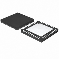
IC TXRX IEEE/ZIGBEE 2.4GHZ 40QFN
Manufacturer
Microchip Technology
Specifications of MRF24J40-I/ML
Package / Case
40-QFN
Frequency
2.4GHz
Data Rate - Maximum
250kbps
Modulation Or Protocol
802.15.4
Applications
ISM, ZigBee™
Power - Output
0dBm
Sensitivity
-95dBm
Voltage - Supply
2.4 V ~ 3.6 V
Current - Receiving
18mA
Current - Transmitting
18mA
Data Interface
PCB, Surface Mount
Antenna Connector
PCB, Surface Mount
Operating Temperature
-40°C ~ 85°C
Number Of Receivers
1
Number Of Transmitters
1
Wireless Frequency
2.4 GHz
Interface Type
4 Wire SPI
Noise Figure
8 dB
Output Power
+ 0 dBm
Operating Supply Voltage
2.5 V, 3.3 V
Maximum Operating Temperature
85 C
Mounting Style
SMD/SMT
Maximum Supply Current
22 mA
Minimum Operating Temperature
- 40 C
Lead Free Status / RoHS Status
Lead free / RoHS Compliant
Memory Size
-
Lead Free Status / Rohs Status
Lead free / RoHS Compliant
Available stocks
Company
Part Number
Manufacturer
Quantity
Price
Company:

Part Number:
MRF24J40-I/ML
Manufacturer:
MICROCHIP
Quantity:
12 000
Part Number:
MRF24J40-I/ML
Manufacturer:
MICROCHIP/微芯
Quantity:
20 000


FIGURE 2-3:
2.8
The 100 kHz internal oscillator requires no external
components and provides one of two Sleep clock
(SLPCLK) frequencies to Sleep mode counters. The
Sleep mode counters time the Beacon Interval (BI) and
inactive period for a beacon-enabled device and the
Sleep interval for a nonbeacon-enabled device. Refer
to Section 3.15 “Sleep” for more information.
The SLPCLK frequency is selectable between the
32 kHz external crystal oscillator or 100 kHz internal
oscillator. The 32 kHz external crystal oscillator
provides better frequency accuracy and stability than
the 100 kHz internal oscillator. It is recommended that
the 100 kHz internal oscillator be calibrated before use.
The calibration procedure is given in Section 3.15.1.2
“Sleep Clock Calibration”.
2.9
An external hardware Reset can be performed by
asserting the RESET pin 13 low. The MRF24J40 will be
released from Reset approximately 250 μs after the
RESET pin is released. The RESET pin has an internal
weak pull-up resistor.
2.10
The Interrupt (INT) pin 16 provides an interrupt signal
to the host microcontroller from the MRF24J40. The
polarity is configured via the INTEDGE bit in the
SLPCON0 (0x211<1>) register. Interrupts have to be
enabled and unmasked before the INT pin is active.
Refer to Section 3.3 “Interrupts” for a functional
description of interrupts.
© 2010 Microchip Technology Inc.
Note:
100 kHz Internal Oscillator
Reset (RESET) Pin
Interrupt (INT) Pin
CL22
CL11
The
0 = Falling Edge. Ensure that the interrupt
polarity matches the interrupt pin polarity
on the host microcontroller.
INTEDGE
32 kHz EXTERNAL
OSCILLATOR CRYSTAL
CIRCUIT
X2
LPOSC2
LPOSC1
polarity
Oscillator
External
32 kHz
Crystal
defaults
Preliminary
to,
2.11
The Wake (WAKE) pin 15 provides an external
wake-up signal to the MRF24J40 from the host micro-
controller. It is used in conjunction with the Sleep
modes of the MRF24J40. The WAKE pin is disabled by
default. Refer to Section 3.15.2 “Immediate Sleep
and Wake-up Mode” for a functional description of the
Immediate Sleep and Wake-up modes.
2.12
Six GPIO pins can be configured individually for control
or monitoring purposes. Input or output selection is
configured by the TRISGPIO (0x34) register. GPIO
data can be read/written to via the GPIO (0x33)
register.
The GPIO pins have limited output drive capability.
Table 2-5 lists the individual GPIO pin source current
limits.
TABLE 2-5:
GPIO0, GPIO1 and GPIO2 can be configured to control
external PA, LNA and RF switches by the internal RF
state machine. This allows the external PA and LNA to
be controlled by the MRF24J40 without any host micro-
controller intervention. Refer to Section 4.2 “External
PA/LNA Control” for control register configuration,
timing diagrams and application information.
Note:
GPIO0
GPIO1
GPIO2
GPIO3
GPIO4
GPIO5
Pin
Wake (WAKE) Pin
General Purpose Input/Output
(GPIO) Pins
The INT pin will remain high or low,
depending on INTEDGE polarity setting,
until INSTAT register is read.
GPIO SOURCE CURRENT
LIMITS
Maximum Current Sourced
MRF24J40
4 mA
1 mA
1 mA
1 mA
1 mA
1 mA
DS39776C-page 11
Related parts for MRF24J40-I/ML
Image
Part Number
Description
Manufacturer
Datasheet
Request
R

Part Number:
Description:
IEEE 802.15.4� 2.4 GHz RF Transceiver
Manufacturer:
MICROCHIP [Microchip Technology]
Datasheet:

Part Number:
Description:
Ieee 802.15.4? 2.4 Ghz Rf Transceiver
Manufacturer:
Microchip Technology Inc.
Datasheet:
Part Number:
Description:
Manufacturer:
Microchip Technology Inc.
Datasheet:
Part Number:
Description:
Manufacturer:
Microchip Technology Inc.
Datasheet:
Part Number:
Description:
Manufacturer:
Microchip Technology Inc.
Datasheet:
Part Number:
Description:
Manufacturer:
Microchip Technology Inc.
Datasheet:
Part Number:
Description:
Manufacturer:
Microchip Technology Inc.
Datasheet:
Part Number:
Description:
Manufacturer:
Microchip Technology Inc.
Datasheet:
Part Number:
Description:
Manufacturer:
Microchip Technology Inc.
Datasheet:
Part Number:
Description:
Manufacturer:
Microchip Technology Inc.
Datasheet: