MRF24J40-I/ML Microchip Technology, MRF24J40-I/ML Datasheet - Page 99
MRF24J40-I/ML
Manufacturer Part Number
MRF24J40-I/ML
Description
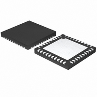
IC TXRX IEEE/ZIGBEE 2.4GHZ 40QFN
Manufacturer
Microchip Technology
Specifications of MRF24J40-I/ML
Package / Case
40-QFN
Frequency
2.4GHz
Data Rate - Maximum
250kbps
Modulation Or Protocol
802.15.4
Applications
ISM, ZigBee™
Power - Output
0dBm
Sensitivity
-95dBm
Voltage - Supply
2.4 V ~ 3.6 V
Current - Receiving
18mA
Current - Transmitting
18mA
Data Interface
PCB, Surface Mount
Antenna Connector
PCB, Surface Mount
Operating Temperature
-40°C ~ 85°C
Number Of Receivers
1
Number Of Transmitters
1
Wireless Frequency
2.4 GHz
Interface Type
4 Wire SPI
Noise Figure
8 dB
Output Power
+ 0 dBm
Operating Supply Voltage
2.5 V, 3.3 V
Maximum Operating Temperature
85 C
Mounting Style
SMD/SMT
Maximum Supply Current
22 mA
Minimum Operating Temperature
- 40 C
Lead Free Status / RoHS Status
Lead free / RoHS Compliant
Memory Size
-
Lead Free Status / Rohs Status
Lead free / RoHS Compliant
Available stocks
Company
Part Number
Manufacturer
Quantity
Price
Company:

Part Number:
MRF24J40-I/ML
Manufacturer:
MICROCHIP
Quantity:
12 000
Part Number:
MRF24J40-I/ML
Manufacturer:
MICROCHIP/微芯
Quantity:
20 000


3.8.1.2
Values of Beacon Order (BO) and Superframe Order
(SO)
Superframe Duration (SD).
Beacon Interval (BI) in terms of BO can be expressed as:
Similarly, Superframe Duration (SD) in terms of SO can
be expressed as:
where aBaseSuperframeduration = 960 symbols.
BO and SO can be configured by programming the BO
(0x10<7:4>) bits and SO (0x10<3:0>) bits in the ORDER
register. For beacon-enabled networks, the values of BO
and SO should be in the range, 0 ≤ SO ≤ BO ≤ 14. If the
values of BO and SO are equal, then the superframe
does not have any inactive portion. A Beacon Interval
can be as short as 15 ms or a long as 251 seconds based
on the values of BO and SO.
FIGURE 3-5:
© 2010 Microchip Technology Inc.
Wait for GTS Slot
Wait for GTS Slot
SD = aBaseSuperframeduration * 2
BI = aBaseSuperframeduration * 2
determine
Transmit Complete
(clear TXG1TRIG)
Transmit Error
BO and SO
Switch TXGTSxFIFO
the
GTSSWITCH = 1
if Transmit Error
or
GTSFIFO STATE DIAGRAM
TXGTS1FIFO
TXGTS2FIFO
Beacon
Interval
Transmit Complete
or
Transmit Error
(clear TXG2TRIG)
(BI)
BO
SO
and
Preliminary
Wait for GTS Slot
Wait for GTS Slot
3.8.1.3
If a device wants to transmit or receive during CFP, it
sends out a “GTS request” in the CAP to the PAN coor-
dinator. The PAN coordinator broadcasts the address
of the device number for that device in the beacon
frame if resources are available.
To
TXGTS1FIFO and TXGTS2FIFO. The TXGTS1FIFO
and TXGTS2FIFO are ping-pong FIFOs and can be
assigned to different GTS slots or to the same slots. If
both are assigned to the same slot, they take turns for
transmission within that slot. TXGTS1FIFO and
TXGTS2FIFO can be triggered ahead of their slot time,
but transmission from the FIFO will take place exactly
at the assigned slot time.
Refer to Section 3.12 “Transmission” for information
on how to transmit a data frame using the
TXGTSxFIFOs.
Hold and wait TXGTSxFIFO
Complete
Transmit
support
GTSSWITCH = 0
if Transmit Error
TXGTS1FIFO
TXGTS2FIFO
GTS
GTS
Transmit
Complete
operation,
MRF24J40
Transmit Error
(clear TXG1TRIG
and TXG2TRIG)
Transmit Error
(clear TXG1TRIG
and TXG2TRIG)
MRF24J40
until Next GTS
Hold and Wait
DS39776C-page 99
uses
Related parts for MRF24J40-I/ML
Image
Part Number
Description
Manufacturer
Datasheet
Request
R

Part Number:
Description:
IEEE 802.15.4� 2.4 GHz RF Transceiver
Manufacturer:
MICROCHIP [Microchip Technology]
Datasheet:

Part Number:
Description:
Ieee 802.15.4? 2.4 Ghz Rf Transceiver
Manufacturer:
Microchip Technology Inc.
Datasheet:
Part Number:
Description:
Manufacturer:
Microchip Technology Inc.
Datasheet:
Part Number:
Description:
Manufacturer:
Microchip Technology Inc.
Datasheet:
Part Number:
Description:
Manufacturer:
Microchip Technology Inc.
Datasheet:
Part Number:
Description:
Manufacturer:
Microchip Technology Inc.
Datasheet:
Part Number:
Description:
Manufacturer:
Microchip Technology Inc.
Datasheet:
Part Number:
Description:
Manufacturer:
Microchip Technology Inc.
Datasheet:
Part Number:
Description:
Manufacturer:
Microchip Technology Inc.
Datasheet:
Part Number:
Description:
Manufacturer:
Microchip Technology Inc.
Datasheet: