MRF24J40-I/ML Microchip Technology, MRF24J40-I/ML Datasheet - Page 7
MRF24J40-I/ML
Manufacturer Part Number
MRF24J40-I/ML
Description
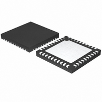
IC TXRX IEEE/ZIGBEE 2.4GHZ 40QFN
Manufacturer
Microchip Technology
Specifications of MRF24J40-I/ML
Package / Case
40-QFN
Frequency
2.4GHz
Data Rate - Maximum
250kbps
Modulation Or Protocol
802.15.4
Applications
ISM, ZigBee™
Power - Output
0dBm
Sensitivity
-95dBm
Voltage - Supply
2.4 V ~ 3.6 V
Current - Receiving
18mA
Current - Transmitting
18mA
Data Interface
PCB, Surface Mount
Antenna Connector
PCB, Surface Mount
Operating Temperature
-40°C ~ 85°C
Number Of Receivers
1
Number Of Transmitters
1
Wireless Frequency
2.4 GHz
Interface Type
4 Wire SPI
Noise Figure
8 dB
Output Power
+ 0 dBm
Operating Supply Voltage
2.5 V, 3.3 V
Maximum Operating Temperature
85 C
Mounting Style
SMD/SMT
Maximum Supply Current
22 mA
Minimum Operating Temperature
- 40 C
Lead Free Status / RoHS Status
Lead free / RoHS Compliant
Memory Size
-
Lead Free Status / Rohs Status
Lead free / RoHS Compliant
Available stocks
Company
Part Number
Manufacturer
Quantity
Price
Company:

Part Number:
MRF24J40-I/ML
Manufacturer:
MICROCHIP
Quantity:
12 000
Part Number:
MRF24J40-I/ML
Manufacturer:
MICROCHIP/微芯
Quantity:
20 000


2.0
2.1
The MRF24J40 is an IEEE 802.15.4 Standard
compliant 2.4 GHz RF transceiver. It integrates the
PHY and MAC functionality in a single chip solution.
Figure 2-1 is a block diagram of the MRF24J40
circuitry.
A frequency synthesizer is clocked by an external
20 MHz crystal and generates a 2.4 GHz RF frequency.
The receiver is a low-IF architecture consisting of a Low
Noise Amplifier (LNA), down conversion mixers, poly-
phase channel filters and baseband limiting amplifiers
with a Receiver Signal Strength Indicator (RSSI).
The transmitter is a direct conversion architecture with
a 0 dBm maximum output (typical) and 36 dB power
control range.
An internal Transmit/Receive (TR) switch combines the
transmitter and receiver circuits into differential RFP
and RFN pins. These pins are connected to impedance
matching circuitry (balun) and antenna. An external
Power Amplifier (PA) and/or LNA can be controlled via
the GPIO pins.
© 2010 Microchip Technology Inc.
HARDWARE DESCRIPTION
2.1 Overview
Preliminary
Six General Purpose Input/Output (GPIO) pins can be
configured for control or monitoring purposes. They
can also be configured to control external PA/LNA RF
switches.
The power management circuitry consists of an
integrated Low Dropout (LDO) voltage regulator. The
MRF24J40 can be placed into a very low-current (2 μA
typical) Sleep mode. An internal 100 kHz oscillator or
32 kHz external crystal oscillator can be used for Sleep
mode timing.
The Media Access Controller (MAC) circuitry verifies
reception and formats for transmission IEEE 802.15.4
Standard compliant packets. Data is buffered in Trans-
mit and Receive FIFOs. Carrier Sense Multiple
Access-Collision Avoidance (CSMA-CA), superframe
constructor, receive frame filter and security engine
functionality are implemented in hardware. The
security engine provides hardware circuitry for
AES-128 with CTR, CCM and CBC-MAC modes.
Control of the transceiver is via a 4-wire SPI, interrupt,
wake and Reset pins.
MRF24J40
DS39776C-page 7
Related parts for MRF24J40-I/ML
Image
Part Number
Description
Manufacturer
Datasheet
Request
R

Part Number:
Description:
IEEE 802.15.4� 2.4 GHz RF Transceiver
Manufacturer:
MICROCHIP [Microchip Technology]
Datasheet:

Part Number:
Description:
Ieee 802.15.4? 2.4 Ghz Rf Transceiver
Manufacturer:
Microchip Technology Inc.
Datasheet:
Part Number:
Description:
Manufacturer:
Microchip Technology Inc.
Datasheet:
Part Number:
Description:
Manufacturer:
Microchip Technology Inc.
Datasheet:
Part Number:
Description:
Manufacturer:
Microchip Technology Inc.
Datasheet:
Part Number:
Description:
Manufacturer:
Microchip Technology Inc.
Datasheet:
Part Number:
Description:
Manufacturer:
Microchip Technology Inc.
Datasheet:
Part Number:
Description:
Manufacturer:
Microchip Technology Inc.
Datasheet:
Part Number:
Description:
Manufacturer:
Microchip Technology Inc.
Datasheet:
Part Number:
Description:
Manufacturer:
Microchip Technology Inc.
Datasheet: