MRF24J40-I/ML Microchip Technology, MRF24J40-I/ML Datasheet - Page 138
MRF24J40-I/ML
Manufacturer Part Number
MRF24J40-I/ML
Description
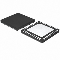
IC TXRX IEEE/ZIGBEE 2.4GHZ 40QFN
Manufacturer
Microchip Technology
Specifications of MRF24J40-I/ML
Package / Case
40-QFN
Frequency
2.4GHz
Data Rate - Maximum
250kbps
Modulation Or Protocol
802.15.4
Applications
ISM, ZigBee™
Power - Output
0dBm
Sensitivity
-95dBm
Voltage - Supply
2.4 V ~ 3.6 V
Current - Receiving
18mA
Current - Transmitting
18mA
Data Interface
PCB, Surface Mount
Antenna Connector
PCB, Surface Mount
Operating Temperature
-40°C ~ 85°C
Number Of Receivers
1
Number Of Transmitters
1
Wireless Frequency
2.4 GHz
Interface Type
4 Wire SPI
Noise Figure
8 dB
Output Power
+ 0 dBm
Operating Supply Voltage
2.5 V, 3.3 V
Maximum Operating Temperature
85 C
Mounting Style
SMD/SMT
Maximum Supply Current
22 mA
Minimum Operating Temperature
- 40 C
Lead Free Status / RoHS Status
Lead free / RoHS Compliant
Memory Size
-
Lead Free Status / Rohs Status
Lead free / RoHS Compliant
Available stocks
Company
Part Number
Manufacturer
Quantity
Price
Company:

Part Number:
MRF24J40-I/ML
Manufacturer:
MICROCHIP
Quantity:
12 000
Part Number:
MRF24J40-I/ML
Manufacturer:
MICROCHIP/微芯
Quantity:
20 000


4.3
The following guidelines are intended to aid users in
high-frequency PCB layout design.
FIGURE 4-5:
• It is important to keep the original PCB thickness
• The first layer width of a 50 Ω characteristic
• Avoid having microstrip lines longer than 2.5 cm,
• Except for the antenna layout, avoid sharp
• Digital lines by definition are prone to be very
DS39776C-page 138
MRF24J40
since any change will affect antenna performance
(see total thickness of dielectric) or microstrip
lines characteristic impedance.
impedance microstrip line is 12 mils.
since that line might get very close to a quarter
wave length of the working frequency of the board
which is 3.0 cm, and start behaving as an
antenna.
corners since they can act as an antenna. Round
corners will eliminate possible future EMI
problems.
noisy when handling periodic waveforms and fast
clock/switching rates. Avoid laying out a RF signal
close to any digital lines.
PCB Layout Design
Note:
FOUR BASIC COPPER FR4 LAYERS
Care should be taken with all ground lines to prevent breakage.
Preliminary
Signal Layout, Thickness = 1.8 mils
Dielectric ε = 4.5, Thickness = 7 mils
RF Ground, Thickness = 1.2 mils
Dielectric ε = 4.5, Thickness = 19 mils
Power Line Routing, Thickness = 1.2 mils
Dielectric ε = 4.5, Thickness = 7 mils
Ground, Thickness = 1.8 mils
The printed circuit board is comprised of four basic FR4
layers: signal layout, RF ground, power line routing and
ground (see Figure 4-5). The guidelines will explain the
requirements of these layers.
• A via filled ground patch underneath the IC
• A power supply must be distributed to each pin in
• Thorough decoupling on each power pin is
• Passive components (inductors) must be in the
transceiver is mandatory.
a star topology and low-ESR capacitors must be
placed at each pin for proper decoupling noise.
beneficial for reducing in-band transceiver noise,
particularly when this noise degrades perfor-
mance. Usually, low value caps (27-47 pF)
combined with large value caps (100 nF) will
cover a large spectrum of frequency.
high-frequency category and the SRF
(Self-Resonant Frequency) should be at least two
times higher than the operating frequency.
© 2010 Microchip Technology Inc.
Related parts for MRF24J40-I/ML
Image
Part Number
Description
Manufacturer
Datasheet
Request
R

Part Number:
Description:
IEEE 802.15.4� 2.4 GHz RF Transceiver
Manufacturer:
MICROCHIP [Microchip Technology]
Datasheet:

Part Number:
Description:
Ieee 802.15.4? 2.4 Ghz Rf Transceiver
Manufacturer:
Microchip Technology Inc.
Datasheet:
Part Number:
Description:
Manufacturer:
Microchip Technology Inc.
Datasheet:
Part Number:
Description:
Manufacturer:
Microchip Technology Inc.
Datasheet:
Part Number:
Description:
Manufacturer:
Microchip Technology Inc.
Datasheet:
Part Number:
Description:
Manufacturer:
Microchip Technology Inc.
Datasheet:
Part Number:
Description:
Manufacturer:
Microchip Technology Inc.
Datasheet:
Part Number:
Description:
Manufacturer:
Microchip Technology Inc.
Datasheet:
Part Number:
Description:
Manufacturer:
Microchip Technology Inc.
Datasheet:
Part Number:
Description:
Manufacturer:
Microchip Technology Inc.
Datasheet: