MRF24J40-I/ML Microchip Technology, MRF24J40-I/ML Datasheet - Page 39
MRF24J40-I/ML
Manufacturer Part Number
MRF24J40-I/ML
Description
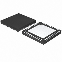
IC TXRX IEEE/ZIGBEE 2.4GHZ 40QFN
Manufacturer
Microchip Technology
Specifications of MRF24J40-I/ML
Package / Case
40-QFN
Frequency
2.4GHz
Data Rate - Maximum
250kbps
Modulation Or Protocol
802.15.4
Applications
ISM, ZigBee™
Power - Output
0dBm
Sensitivity
-95dBm
Voltage - Supply
2.4 V ~ 3.6 V
Current - Receiving
18mA
Current - Transmitting
18mA
Data Interface
PCB, Surface Mount
Antenna Connector
PCB, Surface Mount
Operating Temperature
-40°C ~ 85°C
Number Of Receivers
1
Number Of Transmitters
1
Wireless Frequency
2.4 GHz
Interface Type
4 Wire SPI
Noise Figure
8 dB
Output Power
+ 0 dBm
Operating Supply Voltage
2.5 V, 3.3 V
Maximum Operating Temperature
85 C
Mounting Style
SMD/SMT
Maximum Supply Current
22 mA
Minimum Operating Temperature
- 40 C
Lead Free Status / RoHS Status
Lead free / RoHS Compliant
Memory Size
-
Lead Free Status / Rohs Status
Lead free / RoHS Compliant
Available stocks
Company
Part Number
Manufacturer
Quantity
Price
Company:

Part Number:
MRF24J40-I/ML
Manufacturer:
MICROCHIP
Quantity:
12 000
Part Number:
MRF24J40-I/ML
Manufacturer:
MICROCHIP/微芯
Quantity:
20 000


REGISTER 2-28:
REGISTER 2-29:
REGISTER 2-30:
© 2010 Microchip Technology Inc.
bit 7
Legend:
R = Readable bit
-n = Value at POR
bit 7-4
bit 3-0
bit 7
Legend:
R = Readable bit
-n = Value at POR
bit 7-4
bit 3-0
bit 7
Legend:
R = Readable bit
-n = Value at POR
bit 7-4
bit 3-0
GTS3-3
GTS5-3
R/W-0
R/W-0
R-0
r
GTS3-<3:0>: End Slot of 3rd GTS bits
GTS2-<3:0>: End Slot of 2nd GTS bits
GTS5-<3:0>: End Slot of 5th GTS bits
GTS4-<3:0>: End Slot of 4th GTS bits
Reserved: Maintain as ‘0’
GTS6-<3:0>: End Slot of 6th GTS bits
If 7th GTS exists, the end slot must be 15.
GTS3-2
GTS5-2
R/W-0
R/W-0
ESLOTG23: END SLOT OF GTS3 AND GTS2 REGISTER (ADDRESS: 0x1E)
ESLOTG45: END SLOT OF GTS5 AND GTS4 REGISTER (ADDRESS: 0x1F)
ESLOTG67: END SLOT OF GTS6 REGISTER (ADDRESS: 0x20)
R-0
r
W = Writable bit
‘1’ = Bit is set
W = Writable bit
‘1’ = Bit is set
r = reserved
W = Writable bit
‘1’ = Bit is set
GTS3-1
GTS5-1
R/W-0
R/W-0
R-0
r
GTS3-0
GTS5-0
R/W-0
R/W-0
Preliminary
R-0
r
U = Unimplemented bit, read as ‘0’
‘0’ = Bit is cleared
U = Unimplemented bit, read as ‘0’
‘0’ = Bit is cleared
GTS2-3
GTS4-3
R/W-0
R/W-0
U = Unimplemented bit, read as ‘0’
‘0’ = Bit is cleared
GTS6-3
R/W-0
GTS2-2
GTS4-2
R/W-0
R/W-0
GTS6-2
R/W-0
x = Bit is unknown
x = Bit is unknown
MRF24J40
GTS2-1
GTS4-1
R/W-0
R/W-0
x = Bit is unknown
GTS6-1
R/W-0
DS39776C-page 39
GTS2-0
GTS4-0
R/W-0
R/W-0
GTS6-0
R/W-0
bit 0
bit 0
bit 0
Related parts for MRF24J40-I/ML
Image
Part Number
Description
Manufacturer
Datasheet
Request
R

Part Number:
Description:
IEEE 802.15.4� 2.4 GHz RF Transceiver
Manufacturer:
MICROCHIP [Microchip Technology]
Datasheet:

Part Number:
Description:
Ieee 802.15.4? 2.4 Ghz Rf Transceiver
Manufacturer:
Microchip Technology Inc.
Datasheet:
Part Number:
Description:
Manufacturer:
Microchip Technology Inc.
Datasheet:
Part Number:
Description:
Manufacturer:
Microchip Technology Inc.
Datasheet:
Part Number:
Description:
Manufacturer:
Microchip Technology Inc.
Datasheet:
Part Number:
Description:
Manufacturer:
Microchip Technology Inc.
Datasheet:
Part Number:
Description:
Manufacturer:
Microchip Technology Inc.
Datasheet:
Part Number:
Description:
Manufacturer:
Microchip Technology Inc.
Datasheet:
Part Number:
Description:
Manufacturer:
Microchip Technology Inc.
Datasheet:
Part Number:
Description:
Manufacturer:
Microchip Technology Inc.
Datasheet: