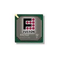
AFS250-FGG256 Actel, AFS250-FGG256 Datasheet - Page 110

AFS250-FGG256
Manufacturer Part Number
AFS250-FGG256
Description
FPGA - Field Programmable Gate Array 250K System Gates
Manufacturer
Actel
Datasheet
1.AFS600-PQG208.pdf
(330 pages)
Specifications of AFS250-FGG256
Processor Series
AFS250
Core
IP Core
Maximum Operating Frequency
1098.9 MHz
Number Of Programmable I/os
114
Data Ram Size
36864
Supply Voltage (max)
1.575 V
Maximum Operating Temperature
+ 70 C
Minimum Operating Temperature
0 C
Development Tools By Supplier
AFS-Eval-Kit, AFS-BRD600, FlashPro 3, FlashPro Lite, Silicon-Explorer II, Silicon-Sculptor 3, SI-EX-TCA
Mounting Style
SMD/SMT
Supply Voltage (min)
1.425 V
Number Of Gates
250 K
Package / Case
FPBGA-256
Lead Free Status / RoHS Status
Lead free / RoHS Compliant
Available stocks
Company
Part Number
Manufacturer
Quantity
Price
Company:
Part Number:
AFS250-FGG256
Manufacturer:
Actel
Quantity:
135
Company:
Part Number:
AFS250-FGG256
Manufacturer:
ACTEL
Quantity:
6 800
Company:
Part Number:
AFS250-FGG256I
Manufacturer:
Microsemi SoC
Quantity:
10 000
- Current page: 110 of 330
- Download datasheet (13Mb)
Device Architecture
Figure 2-75 • Gate Driver
2- 94
Off-Chip
On-Chip
Pads
Power
Gate Driver
The Fusion Analog Quad includes a Gate Driver connected to the Quad's AG pin
Designed to work with external p- or n-channel MOSFETs, the Gate driver is a configurable current sink
or source and requires an external pull-up or pull-down resistor. The AG supports 4 selectable gate drive
levels: 1 µA, 3 µA, 10 µA, and 30 µA
Drive mode in which it can sink 20 mA; in this mode the switching rate is approximately 1.3 MHz with
100 ns turn-on time and 600 ns turn-off time. Modeled on an open-drain-style output, it does not output a
voltage level without an appropriate pull-up or pull-down resistor. If 1 V is forced on the drain, the current
sinking/sourcing will exceed the ability of the transistor, and the device could be damaged.
The AG pad is turned on via the corresponding GDONx pin in the Analog Block macro, where x is the
number of the corresponding Analog Quad for the AG pad to be enabled (GDON0 to GDON9).
The gate-to-source voltage (V
times the external pull-up or pull-down resistor value
The rate at which the gate voltage of the external MOSFET slews is determined by the current, I
sourced or sunk by the AG pin and the gate-to-source capacitance, C
approximation, the slew rate is given by
AV
Prescaler
Digital
Input
Monitor Block
Voltage
(DAVOUTx)
Line Side
To FPGA
To Analog MUX
Monitor / Instr
AC
Prescaler
Amplifier
Digital
Current
Input
gs
) of the external MOSFET is limited to the programmable drive current
Monitor Block
(DACOUTx)
Current
To FPGA
V
Analog Quad
(Figure 2-76 on page
gs
EQ
≤ I
To Analog MUX
g
6.
dv/dt = I
R e visio n 1
R
× (R
pullup
pullup
g
Gate Driver
(EQ
From FPGA
MOSFET
/ C
(GDONx)
Power
or R
GS
5).
AG
pulldown
2-95). The AG also supports a High Current
Driver
Gate
)
GS
, of the external MOSFET. As an
AT
Temperature
Digital
Input
Prescaler
Monitor
Monitor Block
Load Side
Temperature
(DATOUTx)
To FPGA
To Analog MUX
(Figure
2-75).
EQ 5
EQ 6
g
,
Related parts for AFS250-FGG256
Image
Part Number
Description
Manufacturer
Datasheet
Request
R

Part Number:
Description:
FPGA 256/I�/Fusion Voltage: 1.5, 1.8, 2.5, 3.3 Mixed Voltage
Manufacturer:
Actel
Datasheet:

Part Number:
Description:
FPGA - Field Programmable Gate Array 250K System Gates
Manufacturer:
Actel
Datasheet:

Part Number:
Description:
MCU, MPU & DSP Development Tools Silicon Sculptor Programming Mod
Manufacturer:
Actel

Part Number:
Description:
MCU, MPU & DSP Development Tools InSystem Programming ProASICPLUS Devices
Manufacturer:
Actel

Part Number:
Description:
Programming Socket Adapters & Emulators PQ160 Module
Manufacturer:
Actel

Part Number:
Description:
Programming Socket Adapters & Emulators Axcelerator Adap Module Kit
Manufacturer:
Actel

Part Number:
Description:
Programming Socket Adapters & Emulators Evaluation
Manufacturer:
Actel

Part Number:
Description:
Programming Socket Adapters & Emulators AFDX Solutions
Manufacturer:
Actel

Part Number:
Description:
Programming Socket Adapters & Emulators SILICON SCULPTOR ADAPTER MODULE
Manufacturer:
Actel
Datasheet:

Part Number:
Description:
Programming Socket Adapters & Emulators Axcelerator Adap Module Kit
Manufacturer:
Actel

Part Number:
Description:
Programming Socket Adapters & Emulators Evaluation
Manufacturer:
Actel

Part Number:
Description:
Programming Socket Adapters & Emulators Silicon Sculptor Software
Manufacturer:
Actel

Part Number:
Description:
Programming Socket Adapters & Emulators InSystem Programming ProASICPLUS Devices
Manufacturer:
Actel


