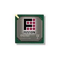
AFS250-FGG256 Actel, AFS250-FGG256 Datasheet - Page 166

AFS250-FGG256
Manufacturer Part Number
AFS250-FGG256
Description
FPGA - Field Programmable Gate Array 250K System Gates
Manufacturer
Actel
Datasheet
1.AFS600-PQG208.pdf
(330 pages)
Specifications of AFS250-FGG256
Processor Series
AFS250
Core
IP Core
Maximum Operating Frequency
1098.9 MHz
Number Of Programmable I/os
114
Data Ram Size
36864
Supply Voltage (max)
1.575 V
Maximum Operating Temperature
+ 70 C
Minimum Operating Temperature
0 C
Development Tools By Supplier
AFS-Eval-Kit, AFS-BRD600, FlashPro 3, FlashPro Lite, Silicon-Explorer II, Silicon-Sculptor 3, SI-EX-TCA
Mounting Style
SMD/SMT
Supply Voltage (min)
1.425 V
Number Of Gates
250 K
Package / Case
FPBGA-256
Lead Free Status / RoHS Status
Lead free / RoHS Compliant
Available stocks
Company
Part Number
Manufacturer
Quantity
Price
Company:
Part Number:
AFS250-FGG256
Manufacturer:
Actel
Quantity:
135
Company:
Part Number:
AFS250-FGG256
Manufacturer:
ACTEL
Quantity:
6 800
Company:
Part Number:
AFS250-FGG256I
Manufacturer:
Microsemi SoC
Quantity:
10 000
- Current page: 166 of 330
- Download datasheet (13Mb)
Device Architecture
2- 15 0
5 V Output Tolerance
Fusion I/Os must be set to 3.3 V LVTTL or 3.3 V LVCMOS mode to reliably drive 5 V TTL receivers. It is
also critical that there be NO external I/O pull-up resistor to 5 V, since this resistor would pull the I/O pad
voltage beyond the 3.6 V absolute maximum value and consequently cause damage to the I/O.
When set to 3.3 V LVTTL or 3.3 V LVCMOS mode, Fusion I/Os can directly drive signals into 5 V TTL
receivers. In fact, VOL = 0.4 V and VOH = 2.4 V in both 3.3 V LVTTL and 3.3 V LVCMOS modes exceed
the VIL = 0.8 V and VIH = 2 V level requirements of 5 V TTL receivers. Therefore, level '1' and level '0'
will be recognized correctly by 5 V TTL receivers.
Simultaneously Switching Outputs and PCB Layout
Any group of four or more input pins switching on the same clock edge is considered an SSO bus. The
shielding should be done both on the board and inside the package unless otherwise described.
In-package shielding can be achieved in several ways; the required shielding will vary depending on
whether pins next to SSO bus are LVTTL/LVCMOS inputs, LVTTL/LVCMOS outputs, or
GTL/SSTL/HSTL/LVDS/LVPECL inputs and outputs. Board traces in the vicinity of the SSO bus have to
be adequately shielded from mutual coupling and inductive noise that can be generated by the SSO bus.
Also, noise generated by the SSO bus needs to be reduced inside the package.
PCBs perform an important function in feeding stable supply voltages to the IC and, at the same time,
maintaining signal integrity between devices.
Key issues that need to considered are as follows:
•
•
•
•
•
Simultaneously switching outputs (SSOs) can produce signal integrity problems on adjacent
signals that are not part of the SSO bus. Both inductive and capacitive coupling parasitics of bond
wires inside packages and of traces on PCBs will transfer noise from SSO busses onto signals
adjacent to those busses. Additionally, SSOs can produce ground bounce noise and V
noise. These two noise types are caused by rapidly changing currents through GND and V
package pin inductances during switching activities:
Ground bounce noise voltage = L(GND) * di/dt
VCCI dip noise voltage = L(VCCI) * di/dt
Power and ground plane design and decoupling network design
Transmission line reflections and terminations
R e visio n 1
CCI
dip
CCI
Related parts for AFS250-FGG256
Image
Part Number
Description
Manufacturer
Datasheet
Request
R

Part Number:
Description:
FPGA 256/I�/Fusion Voltage: 1.5, 1.8, 2.5, 3.3 Mixed Voltage
Manufacturer:
Actel
Datasheet:

Part Number:
Description:
FPGA - Field Programmable Gate Array 250K System Gates
Manufacturer:
Actel
Datasheet:

Part Number:
Description:
MCU, MPU & DSP Development Tools Silicon Sculptor Programming Mod
Manufacturer:
Actel

Part Number:
Description:
MCU, MPU & DSP Development Tools InSystem Programming ProASICPLUS Devices
Manufacturer:
Actel

Part Number:
Description:
Programming Socket Adapters & Emulators PQ160 Module
Manufacturer:
Actel

Part Number:
Description:
Programming Socket Adapters & Emulators Axcelerator Adap Module Kit
Manufacturer:
Actel

Part Number:
Description:
Programming Socket Adapters & Emulators Evaluation
Manufacturer:
Actel

Part Number:
Description:
Programming Socket Adapters & Emulators AFDX Solutions
Manufacturer:
Actel

Part Number:
Description:
Programming Socket Adapters & Emulators SILICON SCULPTOR ADAPTER MODULE
Manufacturer:
Actel
Datasheet:

Part Number:
Description:
Programming Socket Adapters & Emulators Axcelerator Adap Module Kit
Manufacturer:
Actel

Part Number:
Description:
Programming Socket Adapters & Emulators Evaluation
Manufacturer:
Actel

Part Number:
Description:
Programming Socket Adapters & Emulators Silicon Sculptor Software
Manufacturer:
Actel

Part Number:
Description:
Programming Socket Adapters & Emulators InSystem Programming ProASICPLUS Devices
Manufacturer:
Actel


