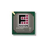
AFS250-FGG256 Actel, AFS250-FGG256 Datasheet - Page 244

AFS250-FGG256
Manufacturer Part Number
AFS250-FGG256
Description
FPGA - Field Programmable Gate Array 250K System Gates
Manufacturer
Actel
Datasheet
1.AFS600-PQG208.pdf
(330 pages)
Specifications of AFS250-FGG256
Processor Series
AFS250
Core
IP Core
Maximum Operating Frequency
1098.9 MHz
Number Of Programmable I/os
114
Data Ram Size
36864
Supply Voltage (max)
1.575 V
Maximum Operating Temperature
+ 70 C
Minimum Operating Temperature
0 C
Development Tools By Supplier
AFS-Eval-Kit, AFS-BRD600, FlashPro 3, FlashPro Lite, Silicon-Explorer II, Silicon-Sculptor 3, SI-EX-TCA
Mounting Style
SMD/SMT
Supply Voltage (min)
1.425 V
Number Of Gates
250 K
Package / Case
FPBGA-256
Lead Free Status / RoHS Status
Lead free / RoHS Compliant
Available stocks
Company
Part Number
Manufacturer
Quantity
Price
Company:
Part Number:
AFS250-FGG256
Manufacturer:
Actel
Quantity:
135
Company:
Part Number:
AFS250-FGG256
Manufacturer:
ACTEL
Quantity:
6 800
Company:
Part Number:
AFS250-FGG256I
Manufacturer:
Microsemi SoC
Quantity:
10 000
- Current page: 244 of 330
- Download datasheet (13Mb)
Device Architecture
2- 22 8
JTAG Pins
Fusion devices have a separate bank for the dedicated JTAG pins. The JTAG pins can be run at any
voltage from 1.5 V to 3.3 V (nominal). VCC must also be powered for the JTAG state machine to operate,
even if the device is in bypass mode; VJTAG alone is insufficient. Both VJTAG and VCC to the Fusion
part must be supplied to allow JTAG signals to transition the Fusion device.
Isolating the JTAG power supply in a separate I/O bank gives greater flexibility with supply selection and
simplifies power supply and PCB design. If the JTAG interface is neither used nor planned to be used,
the VJTAG pin together with the TRST pin could be tied to GND.
TCK
Test clock input for JTAG boundary scan, ISP, and UJTAG. The TCK pin does not have an internal pull-
up/-down resistor. If JTAG is not used, Actel recommends tying off TCK to GND or VJTAG through a
resistor placed close to the FPGA pin. This prevents JTAG operation in case TMS enters an undesired
state.
Note that to operate at all VJTAG voltages, 500 Ω to 1 kΩ will satisfy the requirements. Refer to
Table 2-180
Table 2-180 • Recommended Tie-Off Values for the TCK and TRST Pins
TDI
Serial input for JTAG boundary scan, ISP, and UJTAG usage. There is an internal weak pull-up resistor
on the TDI pin.
TDO
Serial output for JTAG boundary scan, ISP, and UJTAG usage.
TMS
The TMS pin controls the use of the IEEE1532 boundary scan pins (TCK, TDI, TDO, TRST). There is an
internal weak pull-up resistor on the TMS pin.
TRST
The TRST pin functions as an active low input to asynchronously initialize (or reset) the boundary scan
circuitry. There is an internal weak pull-up resistor on the TRST pin. If JTAG is not used, an external pull-
down resistor could be included to ensure the TAP is held in reset mode. The resistor values must be
chosen from
Table 2-180
parallel resistor when multiple devices are connected via a JTAG chain.
In critical applications, an upset in the JTAG circuit could allow entering an undesired JTAG state. In
such cases, Actel recommends tying off TRST to GND through a resistor placed close to the FPGA pin.
Note that to operate at all VJTAG voltages, 500 Ω to 1 kΩ will satisfy the requirements.
VJTAG
VJTAG at 3.3 V
VJTAG at 2.5 V
VJTAG at 1.8 V
VJTAG at 1.5 V
Notes:
1. Equivalent parallel resistance if more than one device is on JTAG chain.
2. The TCK pin can be pulled up/down.
3. The TRST pin can only be pulled down.
for more information.
correspond to the resistor recommended when a single device is used and to the equivalent
Table 2-180
Test Clock
Test Data Input
Test Data Output
Test Mode Select
Boundary Scan Reset Pin
and must satisfy the parallel resistance value requirement. The values in
R e visio n 1
Tie-Off Resistance
200 Ω to 1 kΩ
200 Ω to 1 kΩ
500 Ω to 1 kΩ
500 Ω to 1 kΩ
2, 3
Related parts for AFS250-FGG256
Image
Part Number
Description
Manufacturer
Datasheet
Request
R

Part Number:
Description:
FPGA 256/I�/Fusion Voltage: 1.5, 1.8, 2.5, 3.3 Mixed Voltage
Manufacturer:
Actel
Datasheet:

Part Number:
Description:
FPGA - Field Programmable Gate Array 250K System Gates
Manufacturer:
Actel
Datasheet:

Part Number:
Description:
MCU, MPU & DSP Development Tools Silicon Sculptor Programming Mod
Manufacturer:
Actel

Part Number:
Description:
MCU, MPU & DSP Development Tools InSystem Programming ProASICPLUS Devices
Manufacturer:
Actel

Part Number:
Description:
Programming Socket Adapters & Emulators PQ160 Module
Manufacturer:
Actel

Part Number:
Description:
Programming Socket Adapters & Emulators Axcelerator Adap Module Kit
Manufacturer:
Actel

Part Number:
Description:
Programming Socket Adapters & Emulators Evaluation
Manufacturer:
Actel

Part Number:
Description:
Programming Socket Adapters & Emulators AFDX Solutions
Manufacturer:
Actel

Part Number:
Description:
Programming Socket Adapters & Emulators SILICON SCULPTOR ADAPTER MODULE
Manufacturer:
Actel
Datasheet:

Part Number:
Description:
Programming Socket Adapters & Emulators Axcelerator Adap Module Kit
Manufacturer:
Actel

Part Number:
Description:
Programming Socket Adapters & Emulators Evaluation
Manufacturer:
Actel

Part Number:
Description:
Programming Socket Adapters & Emulators Silicon Sculptor Software
Manufacturer:
Actel

Part Number:
Description:
Programming Socket Adapters & Emulators InSystem Programming ProASICPLUS Devices
Manufacturer:
Actel


