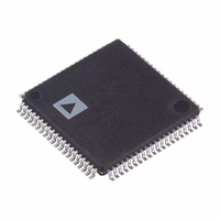
ADV7183BBSTZ Analog Devices Inc, ADV7183BBSTZ Datasheet - Page 13

ADV7183BBSTZ
Manufacturer Part Number
ADV7183BBSTZ
Description
IC,TV/VIDEO CIRCUIT,Color Decoder Circuit,CMOS,QFP,80PIN,PLASTIC
Manufacturer
Analog Devices Inc
Type
Video Decoderr
Datasheet
1.ADV7183BKSTZ.pdf
(100 pages)
Specifications of ADV7183BBSTZ
Applications
Projectors, Recorders, Security
Voltage - Supply, Analog
3.15 V ~ 3.45 V
Voltage - Supply, Digital
1.65 V ~ 2 V
Mounting Type
Surface Mount
Package / Case
80-LQFP
Lead Free Status / RoHS Status
Lead free / RoHS Compliant
Available stocks
Company
Part Number
Manufacturer
Quantity
Price
Company:
Part Number:
ADV7183BBSTZ
Manufacturer:
AD
Quantity:
670
Company:
Part Number:
ADV7183BBSTZ
Manufacturer:
Analog Devices Inc
Quantity:
10 000
ANALOG FRONT END
ANALOG INPUT MUXING
The ADV7183B has an integrated analog muxing section that
allows more than one source of video signal to be connected to
the decoder.
muxing provided in the ADV7183B.
As seen in
by functional registers (INSEL) or manually. Using INSEL[3:0]
simplifies the setup of the muxes and minimizes crosstalk
between channels by pre-assigning the input channels. This is
referred to as ADI recommended input muxing.
Control via an I
ADC0_sw, and ADC1_sw, ADC2_sw) is provided for
applications with special requirements (for example, number/
combinations of signals) that would not be served by the pre-
assigned input connections. This is referred to as manual input
muxing.
F igure 6, the analog input muxes can be controlled
1 4 1 H
F igure 6 outlines the overall structure of the input
1 4 0 H
2
C manual override (ADC_sw_man_en,
ADC_SW_MAN_EN
Figure 6. Internal Pin Connections
Rev. B | Page 13 of 100
AIN1
AIN7
AIN2
AIN8
AIN3
AIN9
AIN4
AIN10
AIN5
AIN11
AIN6
AIN12
AIN3
AIN9
AIN4
AIN10
AIN5
AIN11
AIN6
AIN12
AIN2
AIN8
AIN5
AIN11
AIN6
AIN12
Refer to
controlling the ADV7183B’s input muxing.
ADI Recommended Input Muxing
A maximum of 12 CVBS inputs can be connected and decoded
by the ADV7183B. As seen in
will have to be connected to adjacent pins on the IC. This calls
for a careful design of the PCB layout, such as ground shielding
between all signals routed through tracks that are physically
close together.
INSEL[3:0] Input Selection, Address 0x00[3:0]
The INSEL bits allow the user to select an input channel as well
as the input format. Depending on the PCB connections, only a
subset of the INSEL modes is valid. The INSEL[3:0] not only
switches the analog input muxing, it also configures the
standard definition processor core to process CVBS (Comp),
S-Video (Y/C), or component (YPbPr) format.
1
0
1
0
1
0
F igure 7 for an overview of the two methods of
1 4 2 H
ADC0_SW[3:0]
ADC1_SW[3:0]
ADC2_SW[3:0]
INSEL[3:0]
ADC0
ADC1
ADC2
FUNCTIONS
INTERNAL
MAPPING
F igure 5, this means the sources
1 4 3 H
ADV7183B


