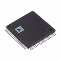
ADV7183BBSTZ Analog Devices Inc, ADV7183BBSTZ Datasheet - Page 16

ADV7183BBSTZ
Manufacturer Part Number
ADV7183BBSTZ
Description
IC,TV/VIDEO CIRCUIT,Color Decoder Circuit,CMOS,QFP,80PIN,PLASTIC
Manufacturer
Analog Devices Inc
Type
Video Decoderr
Datasheet
1.ADV7183BKSTZ.pdf
(100 pages)
Specifications of ADV7183BBSTZ
Applications
Projectors, Recorders, Security
Voltage - Supply, Analog
3.15 V ~ 3.45 V
Voltage - Supply, Digital
1.65 V ~ 2 V
Mounting Type
Surface Mount
Package / Case
80-LQFP
Lead Free Status / RoHS Status
Lead free / RoHS Compliant
Available stocks
Company
Part Number
Manufacturer
Quantity
Price
Company:
Part Number:
ADV7183BBSTZ
Manufacturer:
AD
Quantity:
670
Company:
Part Number:
ADV7183BBSTZ
Manufacturer:
Analog Devices Inc
Quantity:
10 000
ADV7183B
GLOBAL CONTROL REGISTERS
Register control bits listed in this section affect the whole chip.
POWER-SAVE MODES
Power-Down
PDBP, Address 0x0F[2]
The digital core of the ADV7183B can be shut down by using
the PWRDN pin and the PWRDN bit (see below). The PDBP
controls which of the two pins has the higher priority. The
default is to give priority to the PWRDN pin. This allows the
user to have the ADV7183B powered down by default.
When PDBD is 0 (default), the digital core power is controlled
by the PWRDN pin (the bit is disregarded).
When PDBD is 1, the bit has priority (the pin is disregarded).
PWRDN, Address 0x0F[5]
Setting the PWRDN bit switches the ADV7183B into a chip-
wide power-down mode. The power-down stops the clock from
entering the digital section of the chip, thereby freezing its
operation. No I
PWRDN bit also affects the analog blocks and switches them
into low current modes. The I
remains operational in power-down mode.
The ADV7183B leaves the power-down state if the PWRDN
bit is set to 0 (via I
RESET pin.
PDBP must be set to 1 for the PWRDN bit to power down the
ADV7183B.
When PWRDN is 0 (default), the chip is operational.
When PWRDN is 1, the ADV7183B is in chip-wide power-down.
ADC Power-Down Control
The ADV7183B contains three 10-bit ADCs (ADC 0, ADC 1,
and ADC 2). If required, each ADC can be powered down
individually.
The ADCs should be powered down when in:
•
•
CVBS mode. ADC 1 and ADC 2 should be powered down
to save on power consumption.
S-Video mode. ADC 2 should be powered down to save on
power consumption.
2
C bits are lost during power-down. The
2
C), or if the overall part is reset using the
2
C interface is unaffected and
Rev. B | Page 16 of 100
PWRDN_ADC_0, Address 0x3A[3]
When PWRDN_ADC_0 is 0 (default), the ADC is in normal
operation.
When PWRDN_ADC_0 is 1, ADC 0 is powered down.
PWRDN_ADC_1, Address 0x3A[2]
When PWRDN_ADC_1 is 0 (default), the ADC is in normal
operation.
When PWRDN_ADC_1 is 1, ADC 1 is powered down.
PWRDN_ADC_2, Address 0x3A[1]
When PWRDN_ADC_2 is 0 (default), the ADC is in normal
operation.
When PWRDN_ADC_2 is 1, ADC 2 is powered down.
RESET CONTROL
Chip Reset (RES), Address 0x0F[7]
Setting this bit, equivalent to controlling the RESET pin on the
ADV7183B, issues a full chip reset. All I
their default values. (Some register bits do not have a reset value
specified. They keep their last written value. Those bits are
marked as having a reset value of x in the register table.) After
the reset sequence, the part immediately starts to acquire the
incoming video signal.
After setting the RES bit (or initiating a reset via the pin), the
part returns to the default mode of operation with respect to its
primary mode of operation. All I
default values, making this bit self-clearing.
Executing a software reset takes approximately 2 ms. However,
it is recommended to wait 5 ms before any further I
performed.
The I
on the ninth clock cycle when chip reset is implemented. See
the
When RES is 0 (default), operation is normal.
When RES is 1, the reset sequence starts.
M PU Port Description section.
1 4 8 H
2
C master controller receives a no acknowledge condition
2
C bits are loaded with their
2
C registers are reset to
2
C writes are


