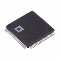
ADV7183BBSTZ Analog Devices Inc, ADV7183BBSTZ Datasheet - Page 26

ADV7183BBSTZ
Manufacturer Part Number
ADV7183BBSTZ
Description
IC,TV/VIDEO CIRCUIT,Color Decoder Circuit,CMOS,QFP,80PIN,PLASTIC
Manufacturer
Analog Devices Inc
Type
Video Decoderr
Datasheet
1.ADV7183BKSTZ.pdf
(100 pages)
Specifications of ADV7183BBSTZ
Applications
Projectors, Recorders, Security
Voltage - Supply, Analog
3.15 V ~ 3.45 V
Voltage - Supply, Digital
1.65 V ~ 2 V
Mounting Type
Surface Mount
Package / Case
80-LQFP
Lead Free Status / RoHS Status
Lead free / RoHS Compliant
Available stocks
Company
Part Number
Manufacturer
Quantity
Price
Company:
Part Number:
ADV7183BBSTZ
Manufacturer:
AD
Quantity:
670
Company:
Part Number:
ADV7183BBSTZ
Manufacturer:
Analog Devices Inc
Quantity:
10 000
ADV7183B
The following sections describe the I
to influence the behavior of the clamps on the ADV7183B.
Previous revisions of the ADV7183B had controls (FACL/FICL,
fast and fine clamp length) to allow configuration of the length
for which the coarse (fast) and fine current sources are switched
on. These controls were removed on the ADV7183B-FT and
replaced by an adaptive scheme.
CCLEN Current Clamp Enable, Address 0x14[4]
The current clamp enable bit allows the user to switch off the
current sources in the analog front end altogether. This can be
useful if the incoming analog video signal is clamped externally.
When CCLEN is 0, the current sources are switched off.
When CCLEN is 1 (default), the current sources are enabled.
DCT[1:0] Digital Clamp Timing, Address 0x15[6:5]
The clamp timing register determines the time constant of the
digital fine clamp circuitry. It is important to realize that the
digital fine clamp reacts very quickly because it is supposed to
immediately correct any residual dc level error for the active
line. The time constant of the digital fine clamp must be much
faster than the one from the analog blocks.
By default, the time constant of the digital fine clamp is adjusted
dynamically to suit the currently connected input signal.
Table 29. DCT Function
DCT[1:0]
00
01
10 (default)
11
DCFE Digital Clamp Freeze Enable, Address 0x15[4]
This register bit allows the user to freeze the digital clamp loop
at any time. It is intended for users who would like to do their
own clamping. Users should disable the current sources for
analog clamping via the appropriate register bits, wait until the
digital clamp loop settles, and then freeze it via the DCFE bit.
When DCFE is 0 (default), the digital clamp is operational.
When DCFE is 1, the digital clamp loop is frozen.
Slow (TC = 1 sec)
Medium (TC = 0.5 sec)
Fast (TC = 0.1 sec)
Determined by the ADV7183B, depending on
the I/P video parameters
Description
2
C signals that can be used
Rev. B | Page 26 of 100
LUMA FILTER
Data from the digital fine clamp block is processed by three sets
of filters. The data format at this point is CVBS for CVBS input
or luma only for Y/C and YPrPb input formats.
•
•
•
F igure 12 through
1 7 4 H
filters together. Unless otherwise noted, the filters are set into a
typical wideband mode.
Luma Antialias Filter (YAA). The ADV7183B receives
video at a rate of 27 MHz. (For 4× oversampled video, the
ADCs sample at 54 MHz, and the first decimation is
performed inside the DPP filters. Therefore, the data rate
into the SDP core is always 27 MHz.) The ITU-R BT.601
recommends a sampling frequency of 13.5 MHz. The luma
antialias filter decimates the oversampled video using a
high quality, linear phase, low-pass filter that preserves the
luma signal while at the same time attenuating out-of-band
components. The luma antialias filter has a fixed response.
Luma Shaping Filters (YSH). The shaping filter block is a
programmable low-pass filter with a wide variety of
responses. It can be used to selectively reduce the luma
video signal bandwidth (needed prior to scaling, for
example). For some video sources that contain high
frequency noise, reducing the bandwidth of the luma
signal improves visual picture quality. A follow-on video
compression stage can work more efficiently if the video is
low-pass filtered.
Digital Resampling Filter. This block is used to allow
dynamic resampling of the video signal to alter parameters
such as the time base of a line of video. Fundamentally, the
resampler is a set of low-pass filters. The actual response is
selected by the system, and user intervention is not
required.
The ADV7183B has two responses for the shaping filter:
one that is used for good quality CVBS, component, and
S-VHS type sources, and a second for nonstandard CVBS
signals.
The YSH filter responses also include a set of notches for
PAL and NTSC. However, using the comb filters for Y/C
separation is recommended.
F igure 15 show the overall response of all
1 7 5 H


