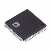
ADV7183BBSTZ Analog Devices Inc, ADV7183BBSTZ Datasheet - Page 57

ADV7183BBSTZ
Manufacturer Part Number
ADV7183BBSTZ
Description
IC,TV/VIDEO CIRCUIT,Color Decoder Circuit,CMOS,QFP,80PIN,PLASTIC
Manufacturer
Analog Devices Inc
Type
Video Decoderr
Datasheet
1.ADV7183BKSTZ.pdf
(100 pages)
Specifications of ADV7183BBSTZ
Applications
Projectors, Recorders, Security
Voltage - Supply, Analog
3.15 V ~ 3.45 V
Voltage - Supply, Digital
1.65 V ~ 2 V
Mounting Type
Surface Mount
Package / Case
80-LQFP
Lead Free Status / RoHS Status
Lead free / RoHS Compliant
Available stocks
Company
Part Number
Manufacturer
Quantity
Price
Company:
Part Number:
ADV7183BBSTZ
Manufacturer:
AD
Quantity:
670
Company:
Part Number:
ADV7183BBSTZ
Manufacturer:
Analog Devices Inc
Quantity:
10 000
Table 75. PAL Line Enable Bits and Corresponding Line
Numbering
Line[3:0]
12
13
14
15
0
1
2
3
4
5
6
7
8
9
10
11
12
13
14
15
0
1
2
3
4
5
6
7
8
9
10
11
IF Compensation Filter
IF FILTSEL[2:0] IF Filter Select Address 0xF8[2:0]
The IF FILTSEL[2:0] register allows the user to compensate for
SAW filter characteristics on a composite input as observed on
tuner outputs.
compensation for NTSC and PAL.
The options for this feature are as follows:
•
•
•
Bypass mode (default)
NTSC—consists of three filter characteristics
PAL—consists of three filter characteristics
Line Number
(ITU-R BT.470)
8
9
10
11
12
13
14
15
16
17
18
19
20
21
22
23
321 (8)
322 (9)
323 (10)
324 (11)
325 (12)
326 (13)
327 (14)
328 (15)
329 (16)
330 (17)
331 (18)
332 (19)
333 (20)
334 (21)
335 (22)
336 (23)
F igure 36 and
2 5 0 H
F igure 37 show IF filter
2 5 1 H
Enable Bit
GDECOL[0]
GDECOL[1]
GDECOL[2]
GDECOL[3]
GDECOL[4]
GDECOL[5]
GDECOL[6]
GDECOL[7]
GDECOL[8]
GDECOL[9]
GDECOL[10]
GDECOL[11]
GDECOL[12]
GDECOL[13]
GDECOL[14]
GDECOL[15]
GDECEL[0]
GDECEL[1]
GDECEL[2]
GDECEL[3]
GDECEL[4]
GDECEL[5]
GDECEL[6]
GDECEL[7]
GDECEL[8]
GDECEL[9]
GDECEL[10]
GDECEL[11]
GDECEL[12]
GDECEL[13]
GDECEL[14]
GDECEL[15]
Comment
Not valid
Not valid
Not valid
Not valid
Not valid
Not valid
Not valid
Not valid
Not valid
Not valid
Not valid
Not valid
Not valid
Not valid
Closed caption
Not valid
Not valid
Not valid
Not valid
Not valid
Not valid
Not valid
Not valid
Not valid
Not valid
Not valid
Not valid
Not valid
Not valid
Not valid
Closed caption
Not valid
Rev. B | Page 57 of 100
See
I
The ADV7183B has a comprehensive interrupt register set. This
map is located in Register Access Page 2. See
of the interrupt register map.
How to access this map is described in
2
P
C Interrupt System
P
ADDRESS 0x0E BIT 6, 5 = 00b
2 5 2 H
REGISTER ACCESS PAGE 1
NORMAL REGISTER SPACE
T able 86 for programming details.
–10
–12
–2
–4
–6
–8
–2
–4
–6
–8
ADDRESS 0x40 ≥ 0xFF
ADDRESS 0x00 ≥ 0x3F
6
4
2
0
6
4
2
0
COMMON I
2.0
3.0
I
2
Figure 36. NTSC IF Compensation Filter Responses
C SPACE
Figure 37. PAL IF Compensation Filter Responses
Figure 38. Register Access —Page 1 and Page 2
2
2.5
3.5
C SPACE
3.0
4.0
FREQUENCY (MHz)
FREQUENCY (MHz)
3.5
4.5
INTERRUPT REGISTER SPACE
ADDRESS 0x0E BIT 6, 5 = 01b
REGISTER ACCESS PAGE 2
ADDRESS 0x40 ≥ 0x4C
F igure 38.
2 5 4 H
4.0
5.0
I
2
C SPACE
T able 84 for details
2 5 3 H
4.5
5.5
ADV7183B
5.0
6.0


