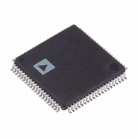
ADV7183BBSTZ Analog Devices Inc, ADV7183BBSTZ Datasheet - Page 25

ADV7183BBSTZ
Manufacturer Part Number
ADV7183BBSTZ
Description
IC,TV/VIDEO CIRCUIT,Color Decoder Circuit,CMOS,QFP,80PIN,PLASTIC
Manufacturer
Analog Devices Inc
Type
Video Decoderr
Datasheet
1.ADV7183BKSTZ.pdf
(100 pages)
Specifications of ADV7183BBSTZ
Applications
Projectors, Recorders, Security
Voltage - Supply, Analog
3.15 V ~ 3.45 V
Voltage - Supply, Digital
1.65 V ~ 2 V
Mounting Type
Surface Mount
Package / Case
80-LQFP
Lead Free Status / RoHS Status
Lead free / RoHS Compliant
Available stocks
Company
Part Number
Manufacturer
Quantity
Price
Company:
Part Number:
ADV7183BBSTZ
Manufacturer:
AD
Quantity:
670
Company:
Part Number:
ADV7183BBSTZ
Manufacturer:
Analog Devices Inc
Quantity:
10 000
DEF_VAL_EN Default Value Enable, Address 0x0C[0]
This bit forces the use of the default values for Y, Cr, and Cb.
Refer to the descriptions for DEF_Y and DEF_C for additional
information. In this mode, the decoder also outputs a stable
27 MHz clock, HS, and VS.
Setting DEF_VAL_EN to 0 (default) outputs a colored screen
determined by user-programmable Y, Cr, and Cb values when
the decoder free-runs. Free-run mode is turned on and off by the
DEF_VAL_AUTO_EN bit.
Setting DEF_VAL_EN to 1 forces a colored screen output
determined by user-programmable Y, Cr, and Cb values. This
overrides picture data even if the decoder is locked.
DEF_VAL_AUTO_EN Default Value Automatic Enable,
Address 0x0C[1]
This bit enables the automatic usage of the default values for
Y, Cr, and Cb when the ADV7183B cannot lock to the
video signal.
Setting DEF_VAL_AUTO_EN to 0 disables free-run mode. If
the decoder is unlocked, it outputs noise.
Setting DEF_VAL_EN to 1 (default) enables free-run mode. A
colored screen set by the user-programmable Y, Cr, and Cb
values is displayed when the decoder loses lock.
CLAMP OPERATION
The input video is ac-coupled into the ADV7183B through a
0.1 μF capacitor. The recommended range of the input video
signal is 0.5 V to 1.6 V (typically 1 V p-p). If the signal exceeds
this range, it cannot be processed correctly in the decoder. Since
the input signal is ac-coupled into the decoder, its dc value
needs to be restored. This process is referred to as clamping the
video. This section explains the general process of clamping on
the ADV7183B and shows the different ways in which a user
can configure its behavior.
The ADV7183B uses a combination of current sources and a
digital processing block for clamping, as shown in
The analog processing channel shown is replicated three times
inside the IC. While only one single channel (and only one
ADC) is needed for a CVBS signal, two independent channels
are needed for Y/C (S-VHS) type signals, and three
independent channels are needed to allow component signals
(YPrPb) to be processed.
ANALOG
VIDEO
INPUT
SOURCES
CURRENT
FINE
F igure 10.
1 7 2 H
COARSE
CURRENT
SOURCES
Figure 10. Clamping Overview
Rev. B | Page 25 of 100
ADC
The clamping can be divided into two sections:
•
•
The ADCs can digitize an input signal only if it resides within
the ADC’s 1.6 V input voltage range. An input signal with a dc
level that is too large or too small is clipped at the top or bottom
of the ADC range.
The primary task of the analog clamping circuits is to ensure
the video signal stays within the valid ADC input window so
that the analog-to-digital conversion can take place. It is not
necessary to clamp the input signal with a very high accuracy in
the analog domain as long as the video signal fits the ADC range.
After digitization, the digital fine clamp block corrects for any
remaining variations in dc level. Since the dc level of an input
video signal refers directly to the brightness of the picture
transmitted, it is important to perform a fine clamp with high
accuracy; otherwise, brightness variations can occur. Further-
more, dynamic changes in the dc level almost certainly lead to
visually objectionable artifacts and must therefore be prohibited.
The clamping scheme has to be able to acquire a newly connected
video signal with a completely unknown dc level, and it must
maintain the dc level during normal operation.
For quickly acquiring an unknown video signal, the large cur-
rent clamps can be activated. (It is assumed that the amplitude
of the video signal at this point is of a nominal value.) Control
of the coarse and fine current clamp parameters is performed
automatically by the decoder.
Standard definition video signals can have excessive noise on
them. In particular, CVBS signals transmitted by terrestrial
broadcast and demodulated using a tuner usually show very
large levels of noise (>100 mV). A voltage clamp is unsuitable
for this type of video signal. Instead, the ADV7183B uses a set
of four current sources that can cause coarse (>0.5 mA) and fine
(<0.1 mA) currents to flow into and away from the high
impedance node that carries the video signal (see
PROCESSOR
CLAMP CONTROL
DATA
(DPP)
Clamping after the ADC (digital domain): digital
processing block
Clamping before the ADC (analog domain): current sources
PRE-
WITH DIGITAL
FINE CLAMP
SDP
ADV7183B
F igure 10).
1 7 3 H


