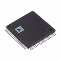
ADV7183BBSTZ Analog Devices Inc, ADV7183BBSTZ Datasheet - Page 15

ADV7183BBSTZ
Manufacturer Part Number
ADV7183BBSTZ
Description
IC,TV/VIDEO CIRCUIT,Color Decoder Circuit,CMOS,QFP,80PIN,PLASTIC
Manufacturer
Analog Devices Inc
Type
Video Decoderr
Datasheet
1.ADV7183BKSTZ.pdf
(100 pages)
Specifications of ADV7183BBSTZ
Applications
Projectors, Recorders, Security
Voltage - Supply, Analog
3.15 V ~ 3.45 V
Voltage - Supply, Digital
1.65 V ~ 2 V
Mounting Type
Surface Mount
Package / Case
80-LQFP
Lead Free Status / RoHS Status
Lead free / RoHS Compliant
Available stocks
Company
Part Number
Manufacturer
Quantity
Price
Company:
Part Number:
ADV7183BBSTZ
Manufacturer:
AD
Quantity:
670
Company:
Part Number:
ADV7183BBSTZ
Manufacturer:
Analog Devices Inc
Quantity:
10 000
MANUAL INPUT MUXING
By accessing a set of manual override muxing registers, the
analog input muxes of the ADV7183B can be controlled
directly. This is referred to as manual input muxing.
Manual input muxing overrides other input muxing control
bits, such as INSEL.
The manual muxing is activated by setting the
ADC_SW_MAN_EN bit. It affects only the analog switches in
front of the ADCs. This means if the settings of INSEL and the
manual input muxing registers (ADC0/ADC1/ADC2_sw)
contradict each other, the ADC0/ADC1/ADC2_sw settings
apply, and INSEL is ignored.
Manual input muxing controls only the analog input muxes.
INSEL[3:0] still has to be set so the follow-on blocks process the
video data in the correct format. This means INSEL must still
be used to tell the ADV7183B whether the input signal is of
component, Y/C, or CVBS format.
Table 10. Manual Mux Settings for All ADCs (SETADC_sw_man_en = 1)
ADC0_sw[3:0]
0000
0001
0010
0011
0100
0101
0110
0111
1000
1001
1010
1011
1100
1101
1110
1111
ADC0 Connected to
No connection
AIN1
AIN2
AIN3
AIN4
AIN5
AIN6
No connection
No connection
AIN7
AIN8
AIN9
AIN10
AIN11
AIN12
No connection
ADC1_sw[3:0]
0000
0001
0010
0011
0100
0101
0110
0111
1000
1001
1010
1011
1100
1101
1110
1111
Rev. B | Page 15 of 100
ADC1 Connected to
No connection
No connection
No connection
AIN3
AIN4
AIN5
AIN6
No connection
No connection
No connection
No connection
AIN9
AIN10
AIN11
AIN12
No connection
Restrictions in the channel routing are imposed by the analog
signal routing inside the IC; every input pin cannot be routed to
each ADC. Refer to
capabilities inside the chip. The three mux sections can be
controlled by the reserved control signal buses ADC0/ADC1/
ADC2_sw[3:0].
SETADC_sw_man_en, Manual Input Muxing Enable,
Address 0xC4[7]
ADC0_sw[3:0], ADC0 mux configuration, Address 0xC3[3:0]
ADC1_sw[3:0], ADC1 mux configuration, Address 0xC3[7:4]
ADC2_sw[3:0], ADC2 mux configuration, Address 0xC4[3:0]
T able 10 explains the control words used.
1 4 7 H
F igure 6 for an overview on the routing
1 4 6 H
ADC2_sw[3:0]
0000
0001
0010
0011
0100
0101
0110
0111
1000
1001
1010
1011
1100
1101
1110
1111
ADC2 Connected to
No connection
No connection
AIN2
No connection
No connection
AIN5
AIN6
No connection
No connection
No connection
AIN8
No connection
No connection
AIN11
AIN12
No connection
ADV7183B


