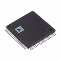
ADV7183BBSTZ Analog Devices Inc, ADV7183BBSTZ Datasheet - Page 18

ADV7183BBSTZ
Manufacturer Part Number
ADV7183BBSTZ
Description
IC,TV/VIDEO CIRCUIT,Color Decoder Circuit,CMOS,QFP,80PIN,PLASTIC
Manufacturer
Analog Devices Inc
Type
Video Decoderr
Datasheet
1.ADV7183BKSTZ.pdf
(100 pages)
Specifications of ADV7183BBSTZ
Applications
Projectors, Recorders, Security
Voltage - Supply, Analog
3.15 V ~ 3.45 V
Voltage - Supply, Digital
1.65 V ~ 2 V
Mounting Type
Surface Mount
Package / Case
80-LQFP
Lead Free Status / RoHS Status
Lead free / RoHS Compliant
Available stocks
Company
Part Number
Manufacturer
Quantity
Price
Company:
Part Number:
ADV7183BBSTZ
Manufacturer:
AD
Quantity:
670
Company:
Part Number:
ADV7183BBSTZ
Manufacturer:
Analog Devices Inc
Quantity:
10 000
ADV7183B
Drive Strength Selection (Clock)
DR_STR_C[1:0] Address 0xF4[3:2]
The DR_STR_C[1:0] bits can be used to select the strength of
the clock signal output driver (LLC pin). For more information,
refer to the
Strength Selection (Data) sections.
Table 12. DR_STR_C Function
DR_STR_C[1:0]
00
01 (default)
10
11
Drive Strength Selection (Sync)
DR_STR_S[1:0] Address 0xF4[1:0]
The DR_STR_S[1:0] bits allow the user to select the strength of
the synchronization signals with which HS, VS, and F are
driven. For more information, refer to the
Selection (Clock) and the
sections.
Table 13. DR_STR_S Function
DR_STR_S[1:0]
00
01 (default)
10
11
D rive Strength Selection (Sync) and the
1 5 7 H
Description
Low drive strength (1×)
Medium low drive strength (2×)
Medium high drive strength (3×)
High drive strength (4×)
Description
Low drive strength (1×)
Medium low drive strength (2×)
Medium high drive strength (3×)
High drive strength (4×)
D rive Strength Selection (Data)
1 6 0 H
D rive Strength
1 5 9 H
D rive
1 5 8 H
Rev. B | Page 18 of 100
Enable Subcarrier Frequency Lock Pin
EN_SFL_PIN Address 0x04[1]
The EN_SFL_PIN bit enables the output of subcarrier lock
information (also known as GenLock) from the ADV7183B to
an encoder in a decoder-encoder back-to-back arrangement.
When EN_SFL_PIN is 0 (default), the subcarrier frequency lock
output is disabled.
When EN_SFL_PIN is 1, the subcarrier frequency lock infor-
mation is presented on the SFL pin.
Polarity LLC Pin
PCLK Address 0x37[0]
The polarity of the clock that leaves the ADV7183B via the
LLC1 and LLC2 pins can be inverted using the PCLK bit.
Changing the polarity of the LLC clock output can be necessary
to meet the setup-and-hold time expectations of follow-on
chips.
This bit also inverts the polarity of the LLC2 clock.
When PCLK is 0, the LLC output polarity is inverted.
When PCLK is 1 (default), the LLC output polarity is normal
(as per the timing diagrams).


